=================================================================================
Pitch doubling through dual patterning has been developed while EUV and high-index fluid-based immersion ArF lithography are not ready for the most aggressive memory designs. [1, 2] Double patterning is essentially an "edge
patterning" process with critical dimension of a line, or space pattern, being defined by the independent position of its
left and right edges. As shown in Figure 2284b, two basic process flows could achieve pitch doubling through double patterning [3]:
i) "Negative" process printing trenches. The negative process prints two trenches in same one hardmask (in orange).
ii) "Positive" process printing lines. The positive process prints 1st line in hardmask and 2nd line in the layer under hardmask.
Figure 2284a shows the process flow of pitch doubling of splitting type. In the second lithographic exposure, the periodical patterns with an offset of half the patten pitch is applied, and thus pitch doubling patterns are obtained. In this method, very precise overlay control is required, because the size of the space patterns is given by the sum of the delineated pattern sizes and overlay error. With this technology, because we can delineate 38 nm half pitch patterns by ArF immersion exposure, and thus by applying double patterning, 19 nm half pitch patterns can be obtained.

| Figure 2284a. Process flow of pitch doubling of splitting type: (a) Cross sectional view showing the line and space patterns and (b) Plain view of 2D layout. [5] |
Five lithographic alternatives, or five mask types, are identified from a darkfield background mask with space structures at 3:1 L/S duty cycle to 1:3 L/S duty cycle on a brightfield mask.
In the "Positive Dual line" flow in Figure 2284b, some characteristics and challenges exist:
i) During Step B, the wafer is
perfectly flat and covered by the hardmask layer.
ii) As shown in Figure 2284c, during Step C, the 2nd patterning takes place on the wafer with topography created by
the patterned hardmask with most of hardmask layer being etched away.
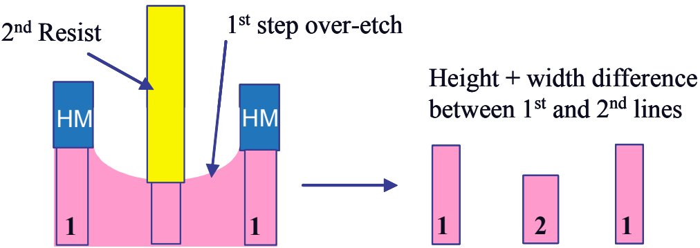
iii) As shown in Figure 2284d, small over-etch during first etch step, could generate a height difference between the
two lines while plasma exposure of the first line during second etch, could add an extra change in CD width.
iv) The main challenge of the process
is the high probability to generate two CD populations since the 1st pattern is going through during the
second etch step because it’s going to be "exposed" to 2nd plasma.
v) Etch-to-litho bias modifies CD mean value as shown in Figure 2284e.
vi) As shown in Figure 2284f, due to the existence of two populations having different mean CD’s, height and profile characteristics, the
difficulty in metrology is to separate population-1 from population-2.

| Figure 2284b. (a) Schematic flows of basic double patterning process options, and (b) Various litho alternatives to achieve pitch doubling for either positive or negative processes. [4] The hardmasks are in orange. |

| Figure 2284c. Difference in Litho 1 and 2, recurring different lith setup and different etch I and II bias. [4] |
| Figure 2284d. Topography and over-etch create two line populations with different line height and width. [4] |
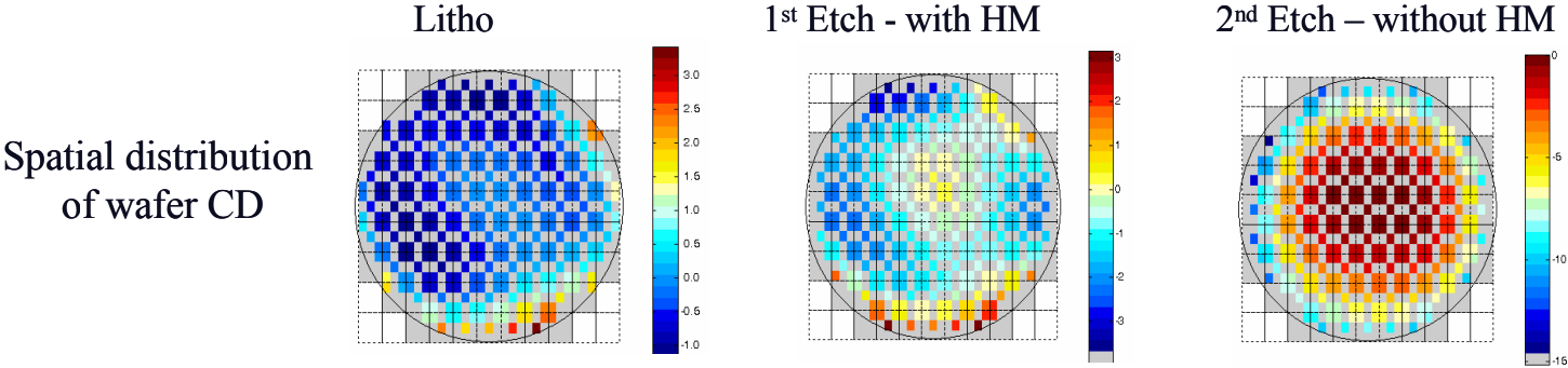
| Figure 2284e. Changes in CD spatial distribution
from litho to etch. 1st and 2nd etch have different distributions. [4] |
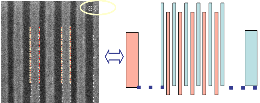
| Figure 2284f. SEM image of a double patterning
structure with lines from one population being highlighted. [4] |
Figure 2284g shows a SEM cross section example of structures produced by splitting-type pitch doubling through dual patterning at different steps.
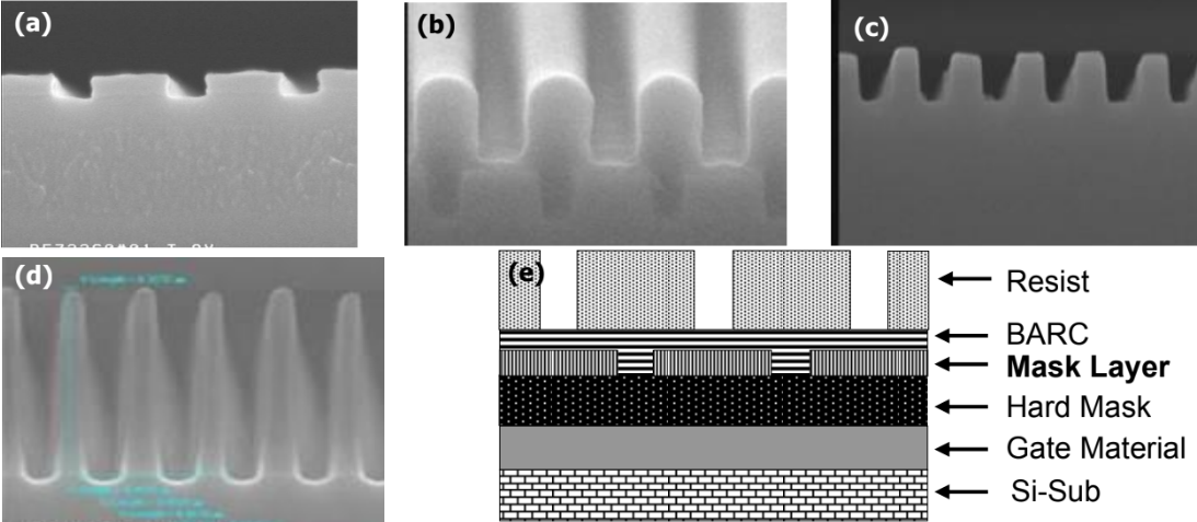
Figure 2284g. SEM cross section view at different steps: (a) after 1st lithography and
etch, (b) after 2nd lithography on patterned topography, (c) after 2nd etching of mask layer, (d) after etching of
main hard mask, (e) schematic diagram of layer structure after 2nd lithography as (b). [6] |
Figure 2284h shows how the target pattern is achieved in negative and positive tone patterning, respectively. Figure 2284i shows SEM images of photo resist and composite pattern of 48 nm flash gate layer. Although the pattern decomposition and optical
proximity correction are different, almost same patterns are achieved by negative and positive tone double patterning processes.

Figure 2284h. De-composite and composite layout of (a) negative tone process and (b) positive tone process. [6] |
|
(a) |
 |
(b) |
Figure 2284i. SEM micrographs of photo resist and composite pattern of 48nm flash gate layer. (a) Negative
tone process, (b) Positive tone process. [6] |
Figure 2284j shows CD asymmetry between adjacent lines due to misalignment between 1st and 2nd lithography patterns.

Figure 2284j. CD asymmetry between adjacent lines: (a) desired pattern in just align case, and (b) CD asymmetry by
misalign between 1st and 2nd lithography patterns. [6] |
Figure 2284k shows the collapse of silicon fins in pitch doubling, published by Kirk Prall.
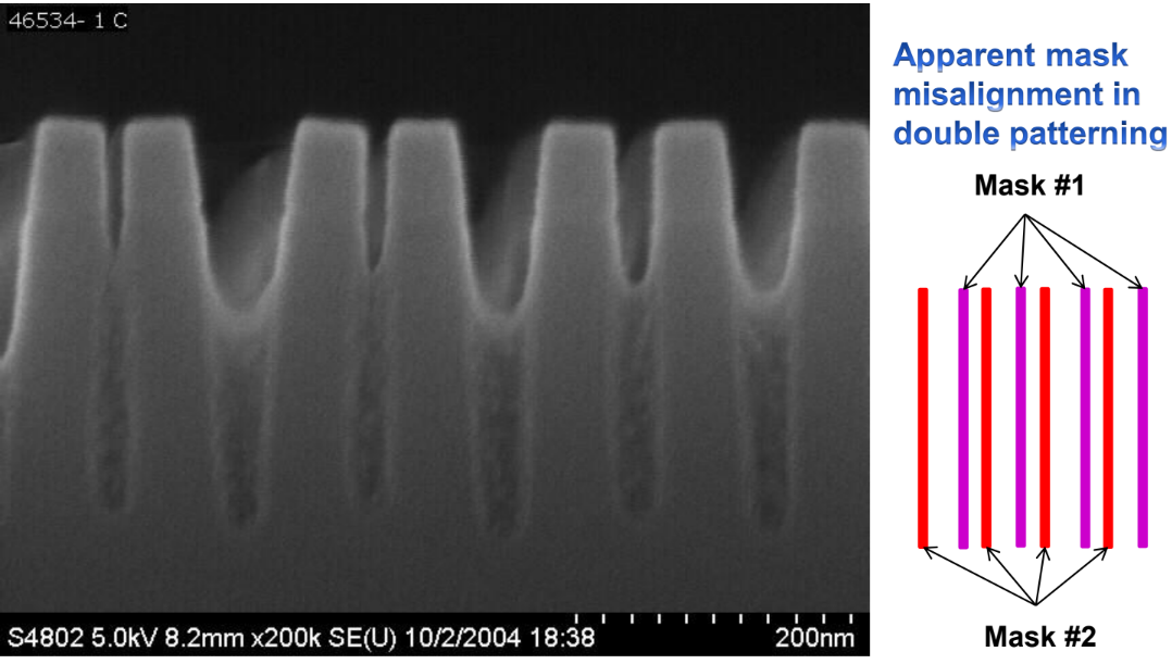
Figure 2284k. Collapse of silicon fins in pitch doubling. [7]
============================================
[1] M. Dusa, W. Arnold, A. Pici, ”prospects and Initial Results from Double Exposure/Double Pitch Technique”,
ISSM2005, San Jose, CA, September 2005.
[2] W. Arnold, M. Dusa, “Manufacturing Challenges in Double Patterning Lithography” ISSM, MC-233, Sept. 2006.
[3] Vincent Wiaux, et all, “193nm Immersion Lithography towards 32nm hp using Double Patterning” 3rd International
Symposium on Immersion Lithography, Kyoto, 2-5 October, 2006.
[4] Mircea Dusa, John Quaedackers, Olaf F. A. Larsen, Jeroen Meessen, Eddy van der Heijden, Gerald Dicker, Onno Wismans, Paul de Haas, Koen van Ingen Schenau, Jo Finders, Bert Vleemingb, Geert Storms, Patrick Jaenen, Shaunee Cheng, Mireille Maenhoudt, Pitch Doubling Through Dual Patterning Lithography Challenges in Integration and Litho Budgets, Proceedings of SPIE - The International Society for Optical Engineering 6520, DOI: 10.1117/12.714278, 2007.
[5] Shinji Okazaki, High resolution optical lithography or high throughput electron beam lithography: The technical struggle from the micro to the nano-fabrication evolution, Microelectronic Engineering 133(8):23-35, DOI: 10.1016/j.mee.2014.11.015, 2015.
[6] Chang-Moon Lim, Seo-Min Kim, Young-Sun Hwang, Jae-Seung Choi, Keun-Do Ban, Sung-Yoon Cho, Jin-Ki Jung, Eung-Kil Kang, Hee-Youl Lim, Hyeong-Soo Kim, and Seung-Chan Moon, Positive and Negative Tone Double Patterning Lithography For 50nm Flash Memory, Optical Microlithography XIX., Proceedings of the SPIE, Volume 6154, pp. 363-370,
DOI: 10.1117/12.656187, (2006).
[7] Kirk Prall, NVSM, 2007.
|
