Sidewall-Spacer-Type Pitch Doubling through Dual/Two Patterning - Integrated Circuits and Materials - - An Online Book - |
||||||||
| Integrated Circuits and Materials http://www.globalsino.com/ICsAndMaterials/ | ||||||||
| Chapter/Index: Introduction | A | B | C | D | E | F | G | H | I | J | K | L | M | N | O | P | Q | R | S | T | U | V | W | X | Y | Z | Appendix | ||||||||
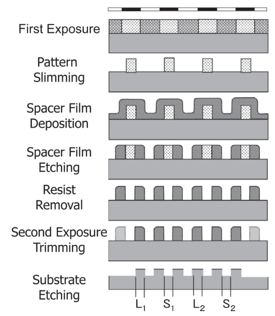
================================================================================= Double patterning is essentially an "edge patterning" process with critical dimension of a line, or space pattern, being defined by the independent position of its left and right edges. [2] Figure 2287b shows process flow of pitch doubling of sidewall spacer type. In this techonique, variations of lines and spaces depends on various parameters. Variations of L1 depend on spacer film thickness variation and etching variation of left sidewall shown by a red arrow. Variations of L2 depend on spacer film thickness variation and etching variation of right sidewall shown by a red arrow. Variations of S1 depend on variations in lithography process and etching variation. Variations of S2 is depend on variations in lithography process, spacer film thickness variation and etching variation.
============================================
[1] Shinji Okazaki, High resolution optical lithography or high throughput electron beam lithography: The technical struggle from the micro to the nano-fabrication evolution, Microelectronic Engineering 133(8):23-35, DOI: 10.1016/j.mee.2014.11.015, 2015.
|
||||||||
| ================================================================================= | ||||||||
|
|
||||||||