=================================================================================
Shallow trench isolation (STI) has been widely used in advanced CMOS technology [2-4] because of:
i) Its superior isolation capability.
ii) Good latch-up immunity.
iii) Suppressed punch-through.
iv) Better surface planarity.
v) Smaller field-oxide encroachment.
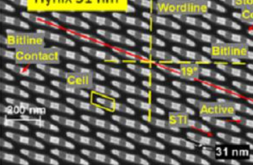
| Figure 2369a. SDRAM array of Hynix 31 nm. The dark contrasts are from STI, while the gray contrasts are from active area of transistors. Adapted from [1] |
However, conventional STI results in "divot"
around the top corner of Si active-area, which leads to:
i) "double hump" in transistor’s Id-vg curves.
ii) Inverse narrow width effect [5, 6].
iii) The defect
and mechanical stress along STI side-wall may enhance
local junction leakage. This is critically important to the data
retention capability (or refresh time TREF) in DRAM [7].
The top corner rounding to avoid "divot" may be enhanced by:
i) High
temperature re-oxidation [8].
ii) Annealing in hydrogen
ambient for Si-migration [9].
iii) STI side-wall oxidation
[10].
iv) A technique of retracted SiN or
"pull-back". [11]
v) A "poly-buffered" STI scheme (
PB-STI) by using SiN/poly-Si/SiO2 stack structure to
form a small oxide bird's beak along STI edge facing
silicon area. [12]
After the 70-nm DRAM node, the STI pitch shrink did not keep pace with the WL pitch shrink until the recessed-channel-array-transistor (RCAT) was introduced by Samsung. RCAT shrunk the STI pitch in the array. (see page2396)
Figure 2369b shows Samsung 48nm 1 Gb DDR3 SDRAM. The active areas are ovals. Each diffusion (active silicon) has two wordlines crossing it. There is a STI gap between all the active areas, such that a third WL does not cross active on this diagonal active direction.
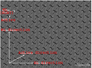
| Figure 2369b. Samsung K4B1G0846F 48nm 1 Gb DDR3 SDRAM,
Poly and Active Area Image under Cell Array.[13] |
Blanket etch process is used in the nitride stripping
process after oxide CMP stops on the nitride layer during STI formation.
============================================
[1] http://www.maltiel-consulting.com/Hynix-DRAM-31Vs44nm-layout.html.
[2] M. Nandakumar, A. Chatterjee, S. Sridhar, K.
Joyner, M. Rodder and I. 4. Chen, “Shallow
trench isolation for advanced ULSI CMOS
technologies,” in IEDMTech. Dig., p. 133, 1998.
[3] K. Kim, C.-G Hwang, and J.G. Lee, “DRAM
technology perspective for gigabit era,” IEEE
Trans. Electron Devices, v.45, no.3, p.598, 1998.
[4] P. VanDerVoorn, D. Gan, and J. P. Krusius,
“CMOS shallow-trench-isolation to 50 nm
channel width,” IEEE Trans. Electron Devices, vol. 47, no. 6, p. 1175,2000.
[5] L. A. Akers, “The inverse-narrow-width effect,”
IEEE Electron Device Lett., vol. 7, 419, 1986.
[6] T. Oishi, K. Shiozawa, A. Furukawa, Y. Abe and Y.
Tokuda, “Isolation edge effect depending on gate
length of MOSFET’s with various isolation
structure,” IEEE Trans. Electron Devices, v.47,
no.4, p.822,2000.
[7] T. Hamamoto, S. Sugiura and S. Sawada, “Well
concentration: A novel scaling limitation factor
derived from DRAM retention time and its
modeling,” in IEDMTech. Dig.. p. 915, 1995.
[8] C. P. Chang et al., “A highly manufacturable comer
rounding solution for 0.18urn shallow trench
isolation,” in IEDMTech. Dig., p661, 1997.
[9] T. Sat0 et al., “Trench transformation technology
using hydrogen annealing for utilizing highly
reliable device structure wil h thin dielectric
films,” in VLSI Tech. Dig., p. 206, 1998.
[10] S. H. Pyi, 1. S. Teo, D. H. Weon, Y. B. Kim, H. S.
Kim and S. K. Lee, “Roles of side-wall oxidation
in the devices with shallow trench isolation,”
IEEE Device Lett., vol. 20, no. 13, p. 384, 1999.
[11] J. Lee, D. Ha and K. Kim, “Novel cell transistor
using retracted Si3N4-liner STI for the
improvement of data retention time in gigabit
density DRAM and beyond,” IEEE Trans.
Electron Devices, vol. 48, no. 6, p. 11 52,2001.
[12] K.Horita, T.Kuroi, Y.Itoh, K.Shiozawa, K.
Eikyu, K.Goto, YInoue and M.Inuishi,
“Advanced shallow trench isolation to suppress
the inverse narrow channel effects for 0.24 um
pitch isolation and beyond,” in VLSI Tech. Dig., p. 178,2000.
[13] http://chipworksrealchips.blogspot.com/2011/01/samsungs-3x-ddr3-sdram-4f2-or-6f2-you.html.
|