=================================================================================
Buried gates in RCAT and BCAT are used to:
i) Mitigate the GIDL.
ii) Mitigate the parasitic capacitance of bit-line.
Figure 2413a shows the channel structure evolution of the cell transistor in dynamic random-access
memory, [5-8] including transmission electron microscope (TEM) images of RCAT, S-RCAT (sphere-shaped RCAT), and U-RCAT (U-shaped RCAT).
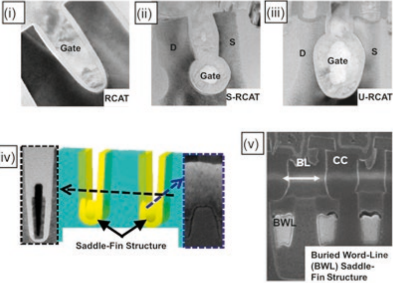
Figure 2413a. Channel structure evolution of the cell transistor in DRAM: Transmission electron microscope (TEM) images of (i) RCAT, (ii) S-RCAT, and
(iii) U-RCAT. (iv) (Middle) Schematic of a saddle-fin transistor with TEM cross-section images
of the (left) x- and (right) y-axes of the transistor. (v) Cross-sectional image of a buried word line
with a saddle-fin channel configuration. [9] |
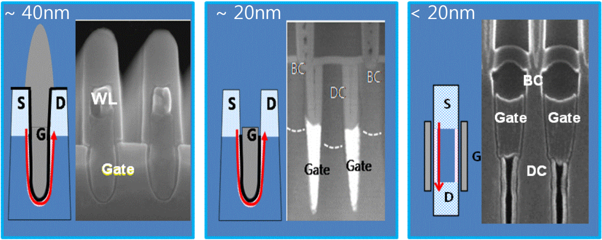
Figure 2413b shows RCAT, BCAT and VCAT. In RCAT and BCAT technologies, the small word-line (WL) metal width is worsened by the non-scalable cell gate oxide thickness. Because VCAT would be free from lateral scaling, it can be one of the best ways to solve the problem.
 |
(a) |
(b) |
(c) |
Figure 2413b. (a) RCAT, (b) BCAT and (c) VCAT. [4]
The STEM images in Figure 2413c show the existence of a bridge defect connecting the gate contact to the
source contact in the indicated panel.
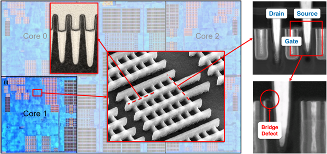
| Figure 2413c. STEM images showing the existence of a bridge defect connecting the gate contact to the
source contact in the indicated panel. [1] |
Figure 2413d shows a buried channel array
transistor (BCAT) in small cell size.

| Figure 2413d. Top view and cross-section TEM images of a buried channel array
transistor (BCAT). [2] |
Ideally,
gate materials in a BCAT have a uniform
depth. However, depths actually differ from each other because of process
variations, as shown in Figure 2413e, resulting in the leakage current distribution. The leakage current (i.e., GIDL) is exponentially proportional to the overlap length between drain node and gate edge (Lov). Figure 2413f shows the experimental results of the relationship between GIDL and Lov in a DRAM cell transistor.
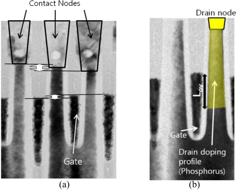
| Figure 2413e. TEM images: (a) Process
variations shown by the double arrows, and (b) Overlap length, Lov, between drain node and gate edge. [3] |
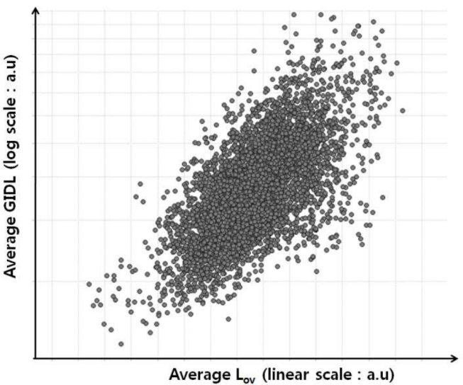
Figure 2413f. Average GIDL increases exponentially with Lov. [3] |
============================================
[1] Jieming Pan, Kain Lu Low, Joydeep Ghosh, Senthilnath Jayavelu, Md Meftahul Ferdaus, Shang Yi Lim, Evgeny Zamburg, Yida Li, Baoshan Tang, Xinghua Wang, Jin Feng Leong, Savitha Ramasamy, Tonio Buonassisi, Chen-Khong Tham, and Aaron Voon-Yew Thean, Transfer Learning-Based Artificial Intelligence-Integrated Physical Modeling to Enable Failure Analysis for 3 Nanometer and Smaller Silicon-Based CMOS Transistors, ACS Appl. Nano Mater., 4, 6903−6915, https://doi.org/10.1021/acsanm.1c00960, 2021.
[2] J. M. Park; Y. S. Hwang; S.-W. Kim; S. Y. Han; J. S. Park; J. Kim; J. W. Seo; B. S. Kim; S. H. Shin; C. H. Cho; S. W. Nam; H. S. Hong, 20 nm DRAM: A new beginning of another revolution, 2015 IEEE International Electron Devices Meeting (IEDM), DOI: 10.1109/IEDM.2015.7409774, 2015.
[3] Min Hee Cho, Namho Jeon, Taek Yong Kim, Moonyoung Jeong, Sungsam Lee, Jong Seo Hong, Hyeong Sun Hong, And Satoru Yamada, An Innovative Indicator to Evaluate DRAM Cell Transistor Leakage Current Distribution, Journal of the Electron Devices Society, 2168-6734, 2017.
[4] Yoosang Hwang, Jemin Park, Gyo-Young Jin, Chilhee Chung, An Overview and Future Challenges of High Density DRAM for 20nm and Beyond, the 2012 International Conference on Solid State Devices and Materials, Kyoto, 2012, pp586-587.
[5] J.V. Kim, H.J. Oh, D.S. Woo, Y.S. Lee, D.H. Kim, S.E. Kim, G.W. Ha, H.J. Kim,
N.J. Kang, J.M. Park, Y.S. Hwang, D.I. Kim, B.J. Park, M. Huh, B.H. Lee,
S.B. Kim, M.H. Cho, M.Y. Jung, Y.I. Kim, C. Jin, D.W. Shin, M.S. Shim, C.S. Lee,
W.S. Lee, J.C. Park, G.Y. Jin, Y.J. Park, K. Kim, Symp. VLSI Technol. Dig. Tech.
Pap. (2005), p. 34.
[6] 5. C. Lee, J.C. Park, S.H. Park, S.S. Lee, S.D. Hong, I.G. Kim, Y.J. Choi, T.W. Lee,
G.Y. Jin, K. Kim, International Conference on Solid State Devices and Materials
(Tsukuba, Japan, 2007), p. 228.
[7] C.M. Yang, C.K. Wei, Y.J. Chang, T.C. Wu, H.P. Chen, C.S. Lai, IEEE Trans.
Device Mater. Reliab. 16, 685 (2016).
[8] T. Schloesser, F. Jakubowski, J.V. Kluge, A. Graham, S. Slesazeck, M. Popp,
P. Baars, K. Muemmler, P. Moll, K. Wilson, A. Buerke, D. Koehler, J. Radecker,
E. Erben, U. Zimmermann, T. Vorrath, B. Fischer, G. Aichmayr, R. Agaiby,
W. Pamler, T. Schster, W. Bergner, W. Mueller, Proc. IEEE Int. Electron Dev. Mtg.
(IEDM) (San Francisco, CA, 2008), p. 1.
[9] Seong Keun Kim and Mihaela Popovici, Future of dynamic random-access memory as main memory, MRS Bulletin , 43(5), Materials for Advanced Semiconductor Memories, pp. 334 - 339, DOI: https://doi.org/10.1557/mrs.2018.95, (2018).
|