Comparison between DiskOnChip, NAND and NOR
- Integrated Circuits and Materials -
- An Online Book -
| Integrated Circuits and Materials http://www.globalsino.com/ICsAndMaterials/ |
Chapter/Index: Introduction | A | B | C | D | E | F | G | H | I | J | K | L | M | N | O | P | Q | R | S | T | U | V | W | X | Y | Z | Appendix
=================================================================================
Table 4186. Comparison between DiskOnChip, NAND and NOR.
| Feature | DiskOnChip | NAND | NOR | |
|---|---|---|---|---|
| =============================== | =============================== | =============================== | ||
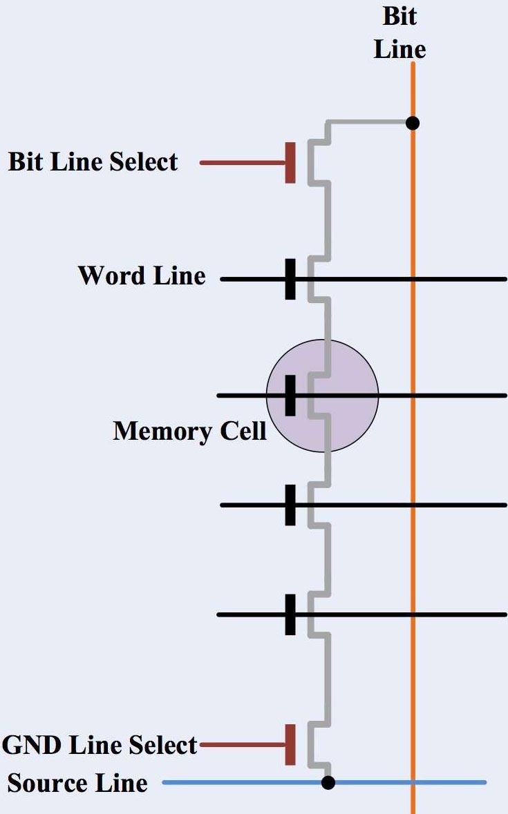
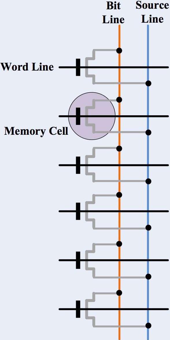
| Memory architecture | A number of memory cells (typically 8 cells) are linked to a series that is identical to a NAND gate | One end of every flash memory cell is linked to the source line; while the other end to a bit line that is identical to a NOR gate | ||
 |
 |
|||
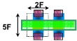
| Layout | 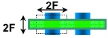 [1] [1] |
 [1] [1] |
||
| Cross-section |  [1] [1] |
 [1] [1] |
||
| Capacity | 8 Mb - 1024 Mb | 8 Mb - 16 Gb. The large capacity is the reason why it is primarily used for the data storage application | 1 MB - 2 Gb; Making its utility within a limited capacity | |
| Density | High: 256 Mb | Low: 32 Mb chips | ||
| Cell size | 4F2 | 10F2 | ||
| Memory range and cell size | Offers a much small cell size and comparatively higher write and erase speed rates | Renders enough address lines that can sufficiently map the whole memory range. That provides an edge of short read times and random access, ensuring it good for code execution | ||
| Sector size | ~ 1 Mb | ~ 1Mb | ||
| Program time | 400 µs/page | 9 µs/word | ||
Cost per bit |
Lower: 2.533x10⁻⁹ USD/bit or $0.25 per Mb | Higher: 6.57x10⁻⁹ USD/bit or $1-$2 per Mb | ||
| Performance | Read/write | Page-oriented | Bitwise | |
| Random read speed | Fast | Slower (30 µs); 25 µs (first byte), 0.03 µs each for remaining 2111 bytes | Faster (120 ns); reading capacity is directly dependent on the size of block of data; the delay in reading is directly propotional to the increase in size. | |
| Sustained read speed (sector basis) | 23 Mb/s (x8) or 37 Mb/s (x16) | 20.5 Mb/s (x8) or 41 Mb/s (x16) | ||
| Read access time | 10-20 µs page "seek" + 50 ns per byte | 50-100 ns | ||
| Read parallelism | 8 - 16 words | 2 Kb | ||
| Write parallelism | 2 kb | 8 - 16 words | ||
| Output parallelism | Byte/word | Byte/word/dword | ||
| Write speed | Fast | Faster: ~300 µs/2112 bytes or 200 µs per page; the data writing can only be done in case a block is empty; similar to read, the writing of data is also done over pages (generally 2 Kb) | Slower: 180 µs/32 bytes, 5 µs per byte; each byte requires to be written along with "0" prior to erase, resulting much slower operation. | |
| Sustained write speed (sector basis) | 5 Mb/s | 0.178 Mb/s | ||
| Erase speed | Fast (3 ms) | Faster (3-3.5 ms), 1 ms/sector, or 2 ms per 16 Kb block; the erase operation is quite straightforward in NAND flash | Slower (520 ms - 5 s), 1 s/sector, or 1 s per 64 Kb block | |
| Erase time per block (typ) | 2 ms | 750 ms | ||
| Erase block size | 128 Kb | 128 Kb | ||
| Programmability | Very limited re-programming | Can modify a single bit | ||
| Power consumption and current | Power on current | Lower (50 mA at max) | Higher (160 mA at max) | |
| Power consumption | Requires less current than NOR flash during initial current flow | During initial power turn on, NOR flash memories need more current | ||
| Standby current | However, in standby mode, it requires more current (1 mA at max) . | However, when put on standby mode, the power consumption is lower (200 µA at max) | ||
| Bit-flipping | More common | Less common | ||
| Bad blocks while shipping | Up to 2% | 0% | ||
| Bad block development | More frequent | Less frequent | ||
| Bad block handling | Mandatory | Not mandatory | ||
| Data retention/life span | At least as high as NAND. Usually much better thanks to TrueFFS | Lower (10 years) | Very high (20 years for 1 K program-erase cycles) | |
| Interface | SRAM-like | I/O only, indirect access, requires toggling both CLE and ALE signals; accessed in bursts of 512 bytes | Full memory interface, random access, SRAM-like, memory mapped | |
| Access | Random on code area | Sequential: Sequential access with a page, or page oriented with spare area on each page | Random | |
| Program-erase cycles | 100,000 - 1,000,000 | Higher (100,000 -1,000,000) | Lower (10,000 - 100,000) | |
| Strengths | More than 10% higher life expectancy | Addressable to every byte | ||
| Good bits | Typically has 98% good bits at the time of shipping with addtional bit falure during the course of the life of the part. That is the reason why it requires ECC (error correcting code) functionality inside the advice | Known to have 100% good bits for the entire life of the part | ||
| Reliability | Extremely high: Built-in EDC/ECC solves bit-flipping. Bad block management supplied by True FFS | Low: Requires at least one bit for error management (bit-flipping issue); bad block management required (needs error correction); bad blocks marked when shipped | Standard: Bit-flipping issues reported less than 10% the life span of NAND; relatively immune to corruption; no bad blocks | |
| Prefered application | XIP boot block | Data/file storage, program, no XIP capacities | XIP capacities (code storage and execution) | |
Table 4811a. Fab flow and properties of DRAM capacitors.
| Reference | ||||||||||||||||||||||||||
|---|---|---|---|---|---|---|---|---|---|---|---|---|---|---|---|---|---|---|---|---|---|---|---|---|---|---|
|
||||||||||||||||||||||||||
| a. |
Table 4834b. xx.
For
|
| [1] https://electronics.stackexchange.com/questions/145358/why-are-nand-flash-and-nor-flash-named-using-the-terms-nand-and-nor. |
=================================================================================