QLC (4 Bits Per Cell) - Integrated Circuits and Materials - - An Online Book - |
||||||||
| Integrated Circuits and Materials http://www.globalsino.com/ICsAndMaterials/ | ||||||||
| Chapter/Index: Introduction | A | B | C | D | E | F | G | H | I | J | K | L | M | N | O | P | Q | R | S | T | U | V | W | X | Y | Z | Appendix | ||||||||
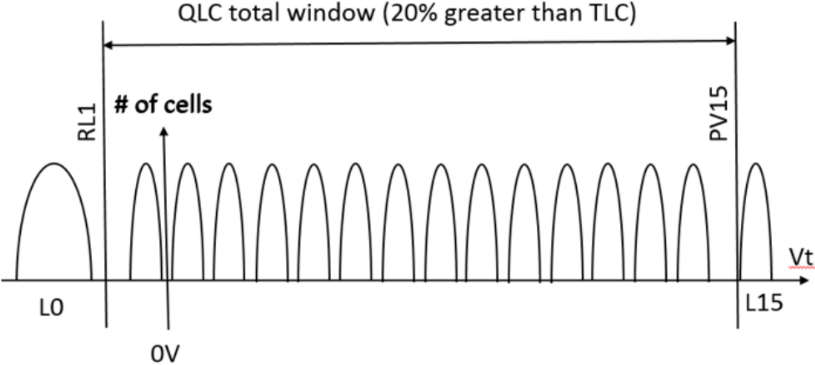
================================================================================= QLC has 4 bits/cell in 16 possible VT states (L0 to L15) as shown in Figure 4199a.
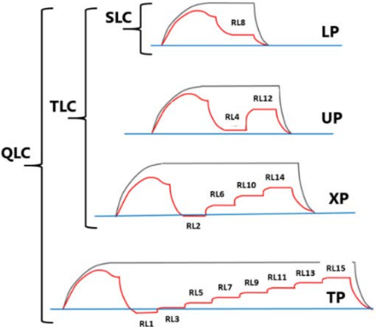
Figure 4199b shows the read sequence for QLC.
A critical issue to enable QLC 3D NAND is the control of Vt distribution width. [1] When using a boosting scheme with uniform Vpass on all WLs, no hot electron (hot-e) injection is usually observed in planar NAND because the non-uniformity of the boosting potential is typically small in a monocrystalline-silicon channel. In 3D NAND, a floating body poly silicon pillar is used, and the lower conductivity of the channel can cause a large voltage drop in the middle of the boosted pillar. This causes hot electron injection in the inner WLs, far from the selectors. Hot electrons can result in severe state width degradation, which hurts QLC applications [2]. A good way to reduce the hot-e distribution is to use asymmetrical seed, which is drain side WLs at a positive voltage and/or the source side WLs at a negative voltage rather than all WLs grounded.
============================================
[1] https://digilander.libero.it/gnaso/articles/tlp/16_1Tb_density_4BPC_3D_NAND_flash_110s_technology.pdf.
|
||||||||
| ================================================================================= | ||||||||
|
|
||||||||