=================================================================================
Figure 4272a shows a DRAM board with an external controller for DDR4 DRAM chips and the DRAM chips.
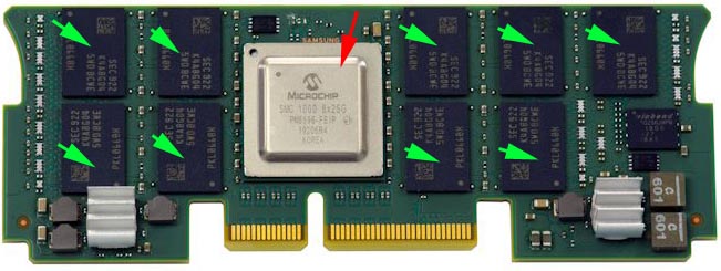
| Figure 4272a. DRAM board with an external controller (pointed by the red arrow) for DDR4 DRAM chips and the DRAM chips (pointed by the green arrows). [1] |
Figure 4272b shows an architecture overview depicting a system with a multi-channel DRAM controller.

Figure 4272b. Architecture overview depicting a system with a multi-channel DRAM controller. [2] |
Figure 4272c shows the data transfer from CPU to DRAM memory in a computer.

Figure 4272c. Data transfer from CPU to DRAM memory in a computer, including an external memory controller. tRCD is indicated by the black arrow. [4] |
As shown in Figure 4272d, tCAS is the delay time between the moment a memory controller tells the memory module to access a particular memory column on a memory module, and the moment the data from given array location is available on the module’s output pin.
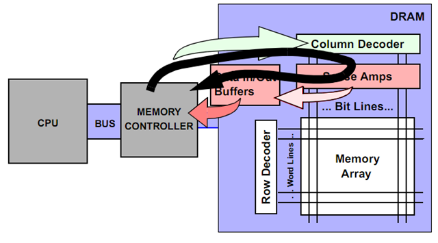
Figure 4272d. tCAS indicated by the black curved arrow. [4]
Table 4272. External DRAM controller parameters on DRAM board. [2]
| Parameter |
Description (unit) |
| Write buffer size |
Number of write queue entries |
| Read buffer size |
Number of read queue entries |
| Write high/low threshold |
High/low watermark for write queue |
| Scheduling policy |
FCFS or FR-FCFS |
| Address mapping |
RoRaBaCoCh, RoRaBaChCo, RoCoRaBaCh [3] |
| Page policy |
Open or closed (adaptive or not) |
| Frontend latency |
Static frontend latency (ns) |
| Backend latency |
Static backend latency (ns) |
| Device bus width |
Data bus with per DRAM device (bits) |
| Burst length |
DRAM burst length (beats) |
| Row-buffer size |
Device row buffer size (bytes) |
| Devices per rank - |
|
| Ranks per channel - |
|
| Banks per rank - |
|
| Channels |
Channel count for the address decoding |
| tRCD |
Row to column delay (ns) |
| tRAS |
Row access strobe (ns) |
| tRP |
Row precharge time (ns) |
| tCL |
Column access latency (ns) |
| tBURST |
Burst duration (ns) |
| tRFC |
Refresh cycle time (ns) |
| tREFI |
Refresh command interval (ns) |
| tWTR |
Write to read switching time (ns) |
| tRRD |
Row to row activation delay (ns) |
| tXAW |
Activation window (ns) |
| Activation limit |
Number of activates in window |
============================================
[1] www.anandtech.com.
[2] Andreas Hansson; Neha Agarwal; Aasheesh Kolli; Thomas Wenisch; Aniruddha N. Udipi, Simulating DRAM controllers for future system architecture exploration, 2014 IEEE International Symposium on Performance Analysis of Systems and Software (ISPASS), DOI: 10.1109/ISPASS.2014.6844484, (2014).
[3] A. B. Kahng and V. Srinivas, “Mobile system considerations
for SDRAM interface trends,” in Proc. SLIP, 2011.
[4] www.cnblogs.com/.
|