=================================================================================
For technologies below 0.18 µm, with lithographic misalignment around 0.1 µm, it becomes the order of the critical dimensions and the alignment precision of the resist masking blocks is no longer sufficient to avoid voids and overlapping. When the voids are transferred into the oxide trench by plasma etching, they are fatal defects for STI. [4]
Table 4519a. Shallow trench isolation (STI) failure mechanisms of CMOS.
| STI |
Test polarity |
Pin pair (stress/reference) |
Failure mechanism |
Failure location |
[1] |
| N+ diffusion diodes |
Positive |
VSS |
Silicide penetration, metallurgical junction, contacts |
Junction surface, Metallurgical junction edge, contact-to-silicon surface |
[1] |
| P+ diffusion diedes |
Positive |
VDD |
Silicon melting, TiSi2 salicide resistance, CoSi2 agglomeration, contact |
N-well under shallow tranch isolation, silicide surface |
[1] |
| N-well diodes |
Negative |
VSS |
Metallurgical junction failure |
|
[1] |
| N-well to n-well |
Negative |
Well-to-well |
Molten silicon |
Shallow trench isolation between wells |
[1] |
| N-channel MOSFET |
Positive |
Drain-to-source |
MOSFET second breakdown |
Molten silicon, MOSFET channel region |
[1] |
| Positive |
Gate |
Gate dielectric failure |
MOSFET gate |
[1] |
| P-channel MOSFET |
Negative |
Drain-to-source |
MOSFET second breakdown |
Molten silicon, MOSFET channel region |
[1] |
Negative
|
MOSFET gate |
Gate dielectric failure |
MOSFET gate |
[1] |
| N-well resistors |
|
|
Resistor second breakdown |
Resistor metallurgical junction, contacts |
[1] |
| N-well ballasted |
Positive |
Drain-to-source |
MOSFET second breakdown |
Molten silicon |
[1] |
| N-channel MOSFET |
Positive
|
Gate |
Gate dielectric failure |
MOSFET channel region and gate |
[1] |
| Aluminum wire interconnect |
Positive |
|
Aluminum melting |
Aluminum film |
[1] |
| Negative |
|
Dielectric cracking |
Aluminum-ILD interface |
[1] |
| Tungsten first level |
Positive |
Signal pin |
ILD (inter-layer-dielectric) breakdown |
Tungsten film-to-polysilicon fill shape, ILD |
[1] |
| Tungsten stud contact |
|
|
Tungsten melting |
Tungsten film, silicon surface |
[1] |
| Tungsten stud bar contact |
Positive |
|
Tungsten melting |
Tungsten film |
[1] |
| Negative |
|
|
Silicon surface |
[1] |
| Copper interconnect |
Positive |
|
Copper melting |
Copper film |
[1] |
| Negative |
|
Dielectric cracking |
Cracking at the Cu-ILD top surface |
[1] |
| Copper via |
Positive |
|
Copper melting |
Copper film |
[1] |
| Negative |
|
|
Cracking at the Cu-ILD top surface |
[1] |
| Copper dual damascene |
Positive |
|
Copper film and via |
Displacement of Cu film and via |
[1] |
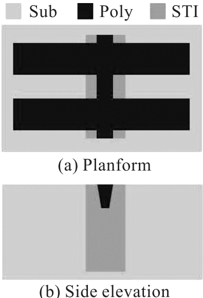
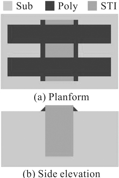
Table 4519b. Poly stringer defects, having three forms. Shallow trench isolation: STI.
| |
STI seams |
STI heights |
STI divots |
| Diagram [2] |
 |
 |
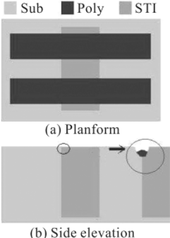 |
| Origin |
Layout dependent, mainly due to the STI width to STI depth ratio (i.e., the aspect ratio) |
STI
chemical mechanical polishing (CMP) processes for different STIs and different active densities [3] |
Wet dip process after the STI CMP but before the poly deposition. |
| More complicated |
Processing conditions such as STI trench etching profiles, gap filling, and poly etching. |
|
|
| Caused failure |
|
|
Causes two poly lines to be short |
[1] Steven H. Voldman, ESD: Failure Mechanisms and Models, 2009.
[2] HU Xiong, PAN Weiwei, SHI Zheng, YAN Xiaolang, MA Tiezhong, Testing Structure for Detection of Poly Stringer Defects in CMOS ICs, TSINGHUA SCIENCE AND TECHNOLOGY, ISSNll1007-0214ll15/17llpp347-351, 15(3), 2010.
[3] Kuei J, Weng Y L. Yield impact from physical design at
advanced technology nodes. In: Proceedings of the 7th
IEEE International Conference on ASIC (ASICON).
Shanghai, China, 2007: 1104-1109.
[4] André Schiltz, Laëtitia Palatini, Maryse Paoli, Maurice Rivoire, and Alain Prola, Plasma etch-back planarization coupled to chemical mechanical polishing for sub 0.18
μm shallow trench isolation technology, Journal of Vacuum Science & Technology A 18, 1313, doi: 10.1116/1.582346, (2000).
|