Failure Analysis Methodology on Resistive Open Defects
- Integrated Circuits - - An Online Book - |
|||||||||||||
| Integrated Circuits http://www.globalsino.com/ICs/ | |||||||||||||
| ================================================================================= | |||||||||||||
Quah et al. [1] had analyzed photoemissions from saturated transistors along a connecting path with open defects in logic arrays. In their analyses, they had employed a combination of techniques, including observation of Photon Emission Microscopy, CAD navigation, layout tracing and EBAC analysis to accurately localize the failure sites. Subtle open defects in advanced technology nodes can be missed because marginal or no leakage signature observable in the power domains. In such cases, the understandings of the common failure signatures related to characteristic wafer map patterns, pattern density correlation and fault localization symptoms associated with different types of defects are very critical in resolving the low yield issues [2]. PFA analysis of such open defects can be classified by the following categories (refer to ICs/page4772):
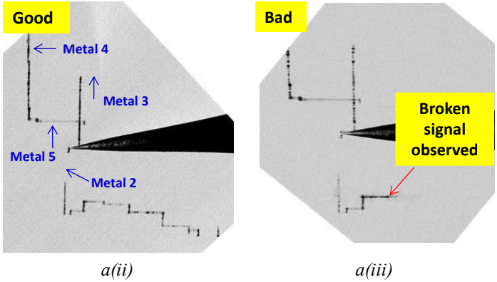
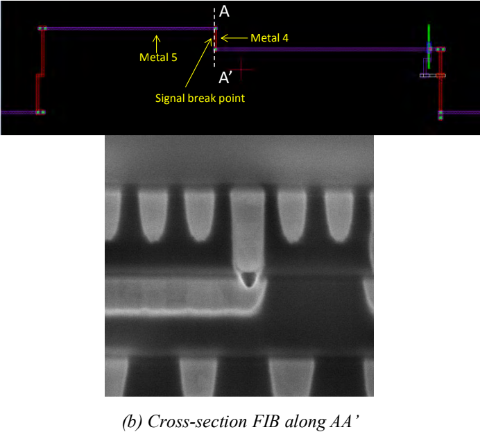
For the case in Figure 4773a (a), Figure 4773b shows an open failure observed with an electron beam at 7 keV by Zyvex Nanoprobing system. The EBAC signal from both metal 5 and metal 4 are observable but electron beam penetration depth is not large enough to observe metal 3. The comparison between good and bad locations showed that there was a signal break on the failed unit which correlated exactly to a metal 5 – metal 4 connection via a single via 4 as shown in the zoom in layout snapshot in Figure 4773b (b). Subsequent FIB cross-section along AA' in Figure 4773b showed via bottom void confirming the suspected open defect.
For the case in Figure 4773a (b), after removing metal 1, the darker contrast in PVC (Passive Voltage Contrast) in Figure 4773c (a) presented at several p+Nwell active contacts. Such spots are verified to be high resistance due to missing contrast as shown in the AFP (AFP (Atomic Force Probing) current imaging in Figure 4773c (b). Figure 4773c (c) shows that the cross-sectional STEM image along BB’ in Figure 4773c (a) indicated that the contact is marginally landed (arrowed in red), where there was insufficient tungsten filling into the silicide contact.
[1] A. C. T. Quah, G. B. Ang, D. Nagalingam, C. Q. Chen, H. P. Ng, S.P. Neo, J. Lam, Z.H. Mai, Failure Analysis Methodology on Resistive Open Defects, ISTFA 2014: Conference Proceedings from the 40th International Symposium for Testing and Failure Analysis, November 9–13, 2014, Houston, Texas, USA.
|
|||||||||||||
| ================================================================================= | |||||||||||||
|
|
|||||||||||||