Electron microscopy
 
Boosted Voltage (VBOOT)
- Integrated Circuits -
- An Online Book -
Integrated Circuits                                                                                   http://www.globalsino.com/ICs/        


=================================================================================


Figure 4882a shows that main-word-lines (MWL0, MWL0B) driven by row decoders is laid out in a two or four times pitch as sub-word-lines. The row decoder and the word-drive decoder include CMOS output gates for the stable operation of main and sub word-lines. Boosted voltage (VBOOT) is supplied to not only word drive decoders but also row decoders to charge the gate of the sub-word-drive-transistor enough to realize the fast decoding even with the small sub-word-drive-transistor. By integrating the decoding circuit and the voltage converter to transform the lower voltage signals into the boosted voltage level. Only the output gate of the word-reset signal-line (MWLOB) is driven at the external voltage (VCC) instead of VBOOT for reduction of the power dissipation.

Main-word-lines (MWL0, MWL0B) driven by row decoders

Figure 4882a. Main-word-lines (MWL0, MWL0B) driven by row decoders. Adapted from [1]. Note that the lines and arrows in red are not real electrical connectors but just indications of the functions of the corresponding sections.

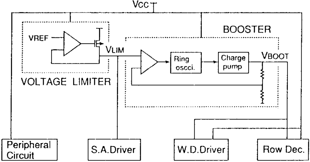
Figure 4882b shows the schematics of a typical power supply of DRAM. There are three voltage levels:
         i) the external voltage (VCC) supplied to most of the peripheral circuits,
         ii) the internal limited voltage (VLIM) supplied to the sense amplifiers,
         iii) the internal boosted voltage (VBOOT) supplied to the row decoders and the word-drive decoders.

Schematics of a typical power supply of DRAM

Figure 4882b. Schematics of a typical power supply of DRAM. [1]. The ring oscillator in the boost circuit is controlled by the comparison of VBOOT with VLIM. so that VBOOT is regulated at a constant level independent of the fluctuation of VCC.


[1] K. Noda, T. Saeki, A. Tsujimoto, T. Murotani, and K. Koyama, "A boosted dual word-line decoding scheme for 256 Mb DRAMs," in 1992 Symposium on VLSI Circuits Digest ofTechnical Papers, pp. 112-113.


=================================================================================