Sub-Wordline Drivers (SWL) - Integrated Circuits - - An Online Book - |
||||||||
| Integrated Circuits http://www.globalsino.com/ICs/ | ||||||||
| ================================================================================= | ||||||||
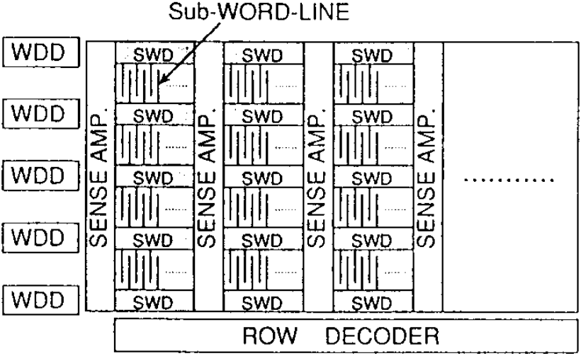
Figure 4889a. Structure of DRAM and peripheral circuitry. [2] In SRAMs, a single word-line is divided into several ones by the sub-wordline drivers (SWD). Every SWD has to be selected by the main word-line (MWL) and the row select line signal (RX). Thus, only a partial word-line will be activated. Figure 4889b shows that SWDs are laid out in place of word-line shunts in conventional array. The SWD selected by a row decoder and a word-drive decoder (WDD) drives the sub-word-line from either side of the cell array.
Figure 4889b. Diagram of dual word-line decoding. [1] Figure 4889c shows that main-word-lines (MWL0, MWL0B) driven by row decoders is laid out in a two or four times pitch as sub-word-lines. The row decoder and the word-drive decoder include CMOS output gates for the stable operation of main and sub word-lines. Boosted voltage (VBOOT) is supplied to not only word drive decoders but also row decoders to charge the gate of the sub-word-drive-transistor enough to realize the fast decoding even with the small sub-word-drive-transistor. By integrating the decoding circuit and the voltage converter to transform the lower voltage signals into the boosted voltage level. Only the output gate of the word-reset signal-line (MWLOB) is driven at the external voltage (VCC) instead of VBOOT for reduction of the power dissipation.
[1] K.Noda, T.Saeki, A.Tsujimoto, T.Murotani, and K.Koyama, A Boosted Dual Word-line Decoding Scheme for 256Mb DRAMs, DOI: 10.1109/VLSIC.1992.229266, (1992).
|
||||||||
| ================================================================================= | ||||||||
|
|
||||||||