Electron microscopy
 
Infrared (IR) Thermography
- Integrated Circuits -
- An Online Book -
Integrated Circuits                                                                                   http://www.globalsino.com/ICs/        


=================================================================================


Infrared (IR) thermography [1-4] is the most popular technique for thermal detection in IC devices. The IR thermography detects an object's temperature from its infrared emission based on blackbody radiation physics [5]. Lock-in thermography (LIT) is the most common used IR thermography in semiconductor industry.

The connection between the peak radiation wavelength and temperature in blackbody theory forms the basis for infrared (IR) temperature measurement.

Most IR thermography systems use one of two types of detectors:
         i) indium antimonide (InSb) detectors, which are sensitive in the wavelength range 1.5 µm to 5.5 µm. Cooled InSb photovoltaics are perhaps the most common detectors for IR thermography.
         ii) mercury cadmium telluride (HgCdTe) detectors, which are sensitive over the range of 8 µm to 12 µm.

Both detectors offer similar temperature sensitivities and ranges, but InSb operates at shorter wavelengths and thus has better spatial resolution. However, in general, IR thermal imaging systems have excellent potential for temperature resolution, but they have a fundamental limitation on spatial resolution (in sub-micron range) due to their long wavelengths.

IR thermal systems rely on directly sensing the emitted infrared radiation from objects to extract their temperature. Systems of this type use a very simple photovoltaic-type detector that is sensitive to IR wavelengths.

The radiance from a sample at a given temperature depends on the radiance that would be collected from a blackbody at the same temperature by the emissivity, [6]
        RT = e•RTBB ---------------------------------------- [4909]
where,
        RT -- the radiance from the sample,
        e -- the sample's emissivity,
        RTBB -- the radiance of a blackbody at the same temperature.

In IC failure analysis, due to the fact that silicon is IR transparent (dependent on its doping concentration), it is possible to investigate the inner structure nondestructively.

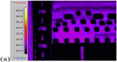
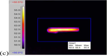
In order to increase the accuracy of the temperature measurement, the radiance that is reflected by the sample must be accounted for. [6] Figure 4909 show that IR systems can easily sense hot areas on integrated circuits with aluminum lines at relatively low power densities but will have difficulty resolving features less than about 5 µm.

IR thermal images of an electro-migration test structure
 
Figure 4909. IR thermal images of an electro-migration test structure: (a) I = 70 mA (actual surface temperature is 36.7 °C), (b) I = 100 mA (actual surface temperature is 52.0 °C, (c) sample coated with black paint, I = 100 mA (actual surface temperature is 55.4 °C). Note (c) was obtained after the surface of the chip was painted with a black non-conductive paint with an emissivity value of 0.96. [6]


[1] Elliott, C. T., Day, D., Wilson, D. J., "An Integrating Detector for Serial Scan Thermal Imaging", Infrared Physics, Vol. 22 (1982). pp. 31-42.
[2] Pote, D., Thome, G., Guthrie, T., "An Overview of Infrared Thermal Imaging Techniques in the Reliability and Failure Analysis of Power Transistors", Proc.14th Intl Symposium for Testing and Failure Analysis (ISTFA), November 1988, pp. 63-75.
[3] Zissis, G. J., "Infrared Technology Fundamentals", Optical Engineering, Vol. 15, No. 6 (1976), pp. 484-497.
[4] Burgraaf, P.,"IR Imaging: Microscopy and Thermography", Semiconductor International, (1986), pp. 5865.
[5] Eisberg, R., and Resnick, R., Quantum Physics, John Wiley and Sons (1974), chapter 1.
[6] Paiboon Tangyunyong and Christian Schmidt, Thermal Defect Detection Techniques, Sandia National Laboratories is a multimission laboratory managed and operated by National Technology & Engineering Solutions of Sandia, LLC, a wholly owned subsidiary of Honeywell International Inc., for the U.S. Department of Energy’s National Nuclear Security Administration under contract DE-NA0003525.


=================================================================================