tRC (Refresh Cycle Time) - Integrated Circuits and Materials - - An Online Book - |
||||||||||||||||||||||||||||||||||||||||||||||||||||||||||||||||||||||||||||||||||
| Integrated Circuits and Materials http://www.globalsino.com/ICsAndMaterials/ | ||||||||||||||||||||||||||||||||||||||||||||||||||||||||||||||||||||||||||||||||||
| ================================================================================= | ||||||||||||||||||||||||||||||||||||||||||||||||||||||||||||||||||||||||||||||||||
A DRAM cell is composed of an access transistor and one leaky capacitor. [2] To prevent data loss due to leakage, DRAM cells require recharge periodically. These recharge operations are also known as DRAM refresh. Two important parameters for DRAM refresh are: Refresh commands are issued by memory controller typically every 7.8μs to refresh a bin, which is composed of multiple rows. That is, the memory controller sends a refresh command to DRAM devices every tREF (7.8 µs normally), and the duration of a refresh command is referred to as tRFC, which means that the refresh operation takes tRFC to complete, which proportionally depends on the number of rows in the bin. The refresh overhead is given by tRFC/tREF, which is the ratio of refresh time to refresh all its cells. Upon receiving REF, DRAM device refresh the designated rows tracked by the internal counter. The whole memory rank is typically refreshed every 64 ms, the vast majority cells can hold data for a much longer time. Table 4937a. Refresh cycle time (tRFC) and refresh overhead (tRFC/tREF) among different density. [2]
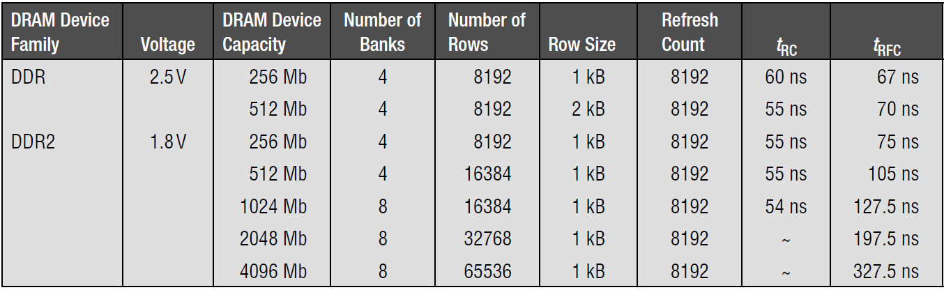
Figure 4937. All-banks-concurrent row refresh timing. [1] Table 4937b. Refresh cycle times for DDR and DDR2 SDRAM devices. [1]
Table 4937c. External DRAM controller parameters on DRAM board. [3]
[1] Bruce Jacob, Spencer W. Ng, and David T. Wang, Memory Systems: Cache, DRAM, Disk, 2008.
|
||||||||||||||||||||||||||||||||||||||||||||||||||||||||||||||||||||||||||||||||||
| ================================================================================= | ||||||||||||||||||||||||||||||||||||||||||||||||||||||||||||||||||||||||||||||||||
|
|
||||||||||||||||||||||||||||||||||||||||||||||||||||||||||||||||||||||||||||||||||