In DRAM, half-VCC voltage is important to maintain a signal-to-noise
ratio because it is applied to: [3]
i) The cell plate to determine the
stored charge.
ii) The data line as the reference voltage for signal detection.
Figure 4957a shows the schematics of a typical power supply of DRAM. There are three voltage levels:
i) the external voltage (VCC) supplied
to most of the peripheral circuits,
ii) the internal limited voltage (VLIM) supplied
to the sense amplifiers,
iii) the internal boosted voltage (VBOOT) supplied to
the row decoders and the word-drive decoders.
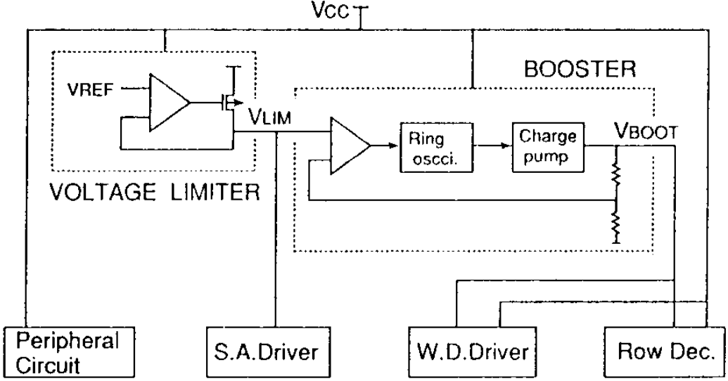
| Figure 4957a. Schematics of a typical power supply of DRAM. [1]. The ring oscillator in the boost circuit is controlled by the comparison of VBOOT with VLIM. so that VBOOT is regulated at a constant level independent of the fluctuation of VCC. |
Figure 4957b
shows that before a row-access operation, the bitline
is precharged, and the voltage on the bitline is set to
the reference voltage, Vref, as well as illustrates the relationship between
two important timing parameters: tRCD and tRAS. In phase one, the wordline
voltage is overdriven to at least Vt above Vcc, and the
DRAM cell discharges the content of the cell onto the bitline and raises the voltage from Vref to
Vref+. In
phase two, the sense control signals SAN and SAP are
activated in quick succession and drive the voltage
on the bitline to the full voltage. Then, the voltage on the
bitline restores the charge in the DRAM cells in
phase three.
Although the relative durations of tRCD and tRAS are not drawn to scale, after
time tRCD, the sensing operation is complete, and
the data can be read out through the DRAM device’s
data I/O. However, after a time period of tRCD from
the beginning of the activation process, data is yet to be restored to the DRAM cells. The data restore operation is completed after a time
period of tRAS from the beginning of the activation
process, and the DRAM device is then ready to accept
a precharge command that will complete the entire
row cycle process after a time period of tRP.
Here, the term definitions are:
Bitline,
Vref ,
tRCD
tRAS
VCC
tRP
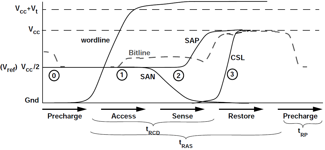
Figure 4957b. Simplified sense amplifier voltage waveform. Read(1) as an example. [2] |
[1] K.Noda, T.Saeki, A.Tsujimoto, T.Murotani, and K.Koyama, A Boosted Dual Word-line Decoding Scheme for 256Mb DRAMs, DOI: 10.1109/VLSIC.1992.229266, (1992).
[2] Bruce Jacob, Spencer W. Ng, and David T. Wang, Memory Systems: Cache, DRAM, Disk, 2008.
[3] Y. Nakagome, H. Tanaka, K. Takeuchi, E. Kume, Y. Watanabe, T. Kaga, Y. Kawamoto, F. Murai, R. Izawa, D. Hisamoto and T. Kisu, An experimental 1.5-V 64-Mb DRAM, IEEE Journal of Solid-State Circuits, 26(4), pp. 465 - 472, 1991.
|
