In 3D NAND flash memory, the source can be referred to using different abbreviations depending on the specific design and manufacturer. Some commonly used abbreviations and terms for the source in 3D NAND are:
- SRC: Source
- SL: Source Line
- SLC: Source Line Contact
- SSL: String Source Line
- CSL: Common Source Line
Each of these abbreviations can be used interchangeably to refer to the source in the memory array, but their usage may vary based on specific technical documentation, design conventions, and the manufacturer’s terminology.
However, SSL and CSL do not represent the exact same thing in 3D NAND flash memory:
- SSL (String Source Line):
- SSL refers to the source line that is specific to a single string of memory cells.
- In a NAND flash memory array, each string (a series of memory cells connected in series) has its own source line, connecting the source terminals of all transistors in that particular string.
- SSL is more localized and pertains to individual strings within the memory array.
- CSL (Common Source Line):
- CSL refers to a common source line that serves as a shared source connection for multiple strings of memory cells.
- It is a more global connection within the memory array that connects the source terminals of transistors from several strings.
- CSL helps in simplifying the layout and reducing the number of individual source lines needed by sharing the source connection across multiple strings.
- Contextual Usage:
- SSL is typically used when discussing the source line specific to each string.
- CSL is used when referring to a shared or common source line that serves multiple strings, simplifying the overall design and routing within the 3D NAND structure.
The number of sources in an SSL (String Source Line) is not the same as the number of sources in a CSL (Common Source Line):
- SSL (String Source Line):
- An SSL is dedicated to a single string of memory cells.
- Each string in a NAND array has its own source line connecting the source terminals of all the transistors in that string.
- Therefore, the number of sources in an SSL is equal to the number of memory cells (or transistors) in that specific string.
- CSL (Common Source Line):
- A CSL serves as a shared source connection for multiple strings of memory cells.
- It aggregates the source terminals from several strings into a common line.
- Consequently, the number of sources connected to a CSL is the sum of the sources from all the strings it serves.
- Example:
- SSL: If a string contains 32 memory cells, then an SSL for that string has 32 sources.
- CSL: If a CSL connects 4 strings, each with 32 memory cells, then the CSL has 4 * 32 = 128 sources.
In 3D NAND flash memory, a Column-Select Line (CSL) is an essential component in the architecture that helps manage and control access to memory cells within a block:
- Purpose:
- The CSL is used to select specific columns (bit lines) within the memory array for reading or writing operations. It ensures that data can be accessed or modified accurately at the desired location.
- Architecture:
- In a typical 3D NAND structure, memory cells are stacked vertically, creating a 3D array. Each layer of this array has multiple word lines (WLs) and bit lines (BLs).
- The CSL runs perpendicular to the word lines and bit lines, allowing it to interface with the vertical stack of memory cells.
- Operation:
- During a read or write operation, the CSL is activated to connect a specific column of memory cells to the sense amplifiers or the write circuitry.
- It works in conjunction with word lines (which select the rows) and bit lines (which connect the cells to sense amplifiers or write circuits).
- Control:
- The CSL is controlled by the memory controller, which sends signals to activate the appropriate column for the desired operation. This control ensures that only the selected column's data is accessed or modified, maintaining data integrity.
- Design Considerations:
- Designing the CSL involves ensuring minimal interference with adjacent columns and maintaining the signal integrity to avoid errors during high-speed read/write operations.
- Proper isolation and shielding techniques are often employed to minimize cross-talk and other forms of electrical noise.
- Integration in 3D NAND:
- In the 3D NAND architecture, CSLs are part of the peripheral circuitry that interfaces with the vertical array of memory cells. Their design and implementation are crucial for the overall performance and reliability of the memory device.
Figures 4958a shows cross-section view and equivalent circuit diagram of 3D NAND flash array structure.
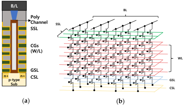
| Figures 4958a. .(a) Cross-section view and (b) equivalent circuit diagram of 3D NAND flash array structure. [7] |
Figures 4958b and 4958c show the SSL (Source Select Line) and CSL in 3D NAND.

| Figure 4958b. (Left) Cross-sectional view and (Right) top layout view of the 3D stacked NAND string. GSL and SSL are the BLS and SLS, respectively. CSL is the common source line. [4, 5] |

Figure 4958c. SSL (Source Select Line) and CSL in 3D NAND. [6] |
This CSL
signal triggers that data transfers between BLs and I/O lines
controlled by the column address. [2]
Figure 4958d shows a diagram of a basic sense amplifier. More complex sense amplifiers in modern DRAM devices contain the basic elements, as well as additional circuit
elements for array isolation, careful balance of the sense amplifier structure, and faster sensing capability. In Figure 4958c, the equalization (EQ) signal line controls the voltage equalization circuit. The functionality of this circuit is to ensure that the voltages on the bitline pairs are as closely matched as possible. Since the differential sense amplifier is designed to amplify the voltage differential between the bitline pairs, thus any voltage imbalance that exists on the bitline pairs prior to the activation of the access transistors would degrade the effectiveness of the sense amplifier. [1] The column-select line (CSL) turns on the output transistors and allows the
fully driven voltage to reach the output and be read
out of the DRAM device.
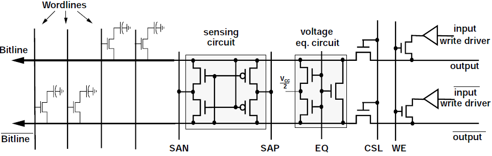
Figure 4958d. Diagram of a basic sense amplifier. [1]
Figure 4958e
shows that before a row-access operation, the bitline
is precharged, and the voltage on the bitline is set to
the reference voltage, Vref, as well as illustrates the relationship between
two important timing parameters: tRCD and tRAS. In phase one, the wordline
voltage is overdriven to at least Vt above Vcc, and the
DRAM cell discharges the content of the cell onto the bitline and raises the voltage from Vref to
Vref+. In
phase two, the sense control signals SAN and SAP are
activated in quick succession and drive the voltage
on the bitline to the full voltage. Then, the voltage on the
bitline restores the charge in the DRAM cells in
phase three.
Although the relative durations of tRCD and tRAS
are not drawn to scale, after
time tRCD, the sensing operation is complete, and
the data can be read out through the DRAM device’s
data I/O. However, after a time period of tRCD from
the beginning of the activation process, data is yet to be restored to the DRAM cells. The data restore operation is completed after a time
period of tRAS from the beginning of the activation
process, and the DRAM device is then ready to accept
a precharge command that will complete the entire
row cycle process after a time period of tRP.
Here, the term definitions are:
Bitline,
Vref ,
tRCD
tRAS
VCC
tRP
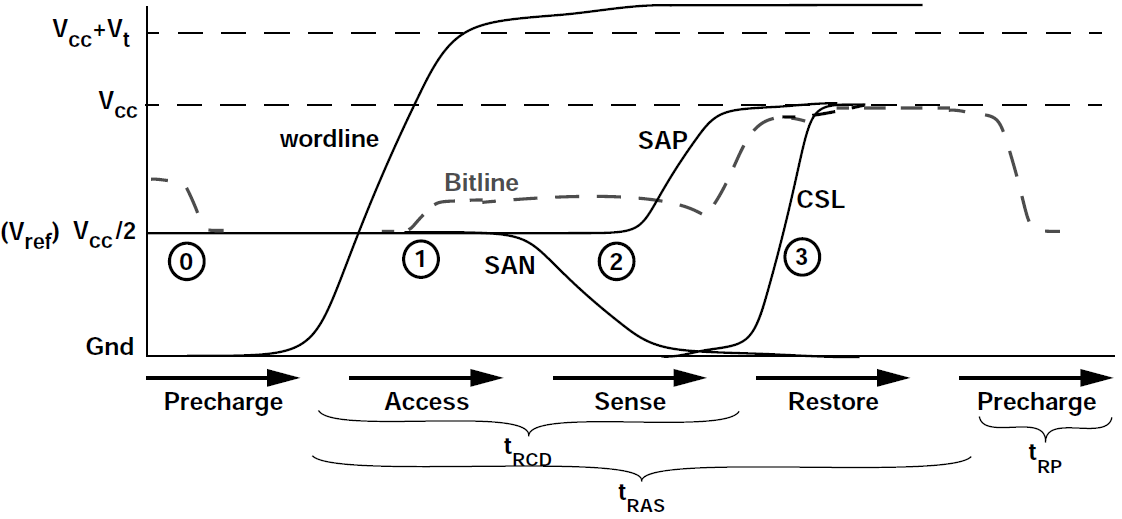
Figure 4958e. Simplified sense amplifier voltage waveform. Read(1) as an example. [1] |
As shown in Figures 4958f, a typical bitline sense-amplifier stripe has 11 transistors per bitline pair. The share of bitline sense-amplifier area to total die area in a typical DRAM die is between 8% and 15%.
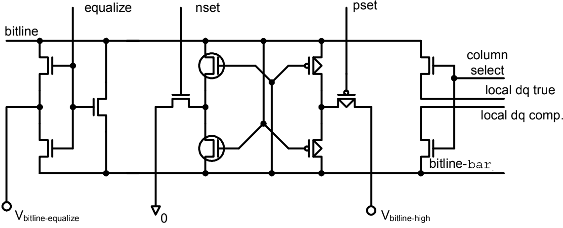
Figure 4958f. Bitline sense-amplifier. [3] |
[1] Bruce Jacob, Spencer W. Ng, and David T. Wang, Memory Systems: Cache, DRAM, Disk, 2008.
[2] Alessio Spessot and Hyungrock Oh, 1T-1C Dynamic Random Access Memory Status, Challenges, and Prospects, IEEE TRANSACTIONS ON ELECTRON DEVICES, 67(4), 1382, 2020.
[3] Thomas Vogelsang, Understanding the Energy Consumption of Dynamic Random Access Memories, 2010 43rd Annual IEEE/ACM International Symposium on Microarchitecture, DOI: 10.1109/MICRO.2010.42, 2010.
[4] https://www.mdpi.com/2073-431X/6/3/27.
[5] Park, K.T.; Kang, M.; Hwang, S.; Kim, D.; Cho, H.; Jeong, Y.; Seo, Y.I.; Jang, J.; Kim, H.S.; Lee, Y.T.; et al. A Fully Performance Compatible 45 nm 4-Gigabit Three Dimensional Double-Stacked Multi-Level NAND Flash Memory with Shared Bit-Line Structure. IEEE J. Solid State Circuit 2009, 44, 208–216.
[6] https://osalesov.best/product_details/37988558.html.
[7] Geun Ho Lee, Sungmin Hwang, Junsu Yu and Hyungjin Kim, Architecture and Process Integration Overview of 3D NAND Flash Technologies, Appl. Sci. 2021, 11, 6703. https://doi.org/10.3390/app11156703.
|