|
||||||||
Wordline (WL) Drivers (WLDVs) - Integrated Circuits and Materials - - An Online Book - |
||||||||
| Integrated Circuits and Materials http://www.globalsino.com/ICsAndMaterials/ | ||||||||
| ================================================================================= | ||||||||
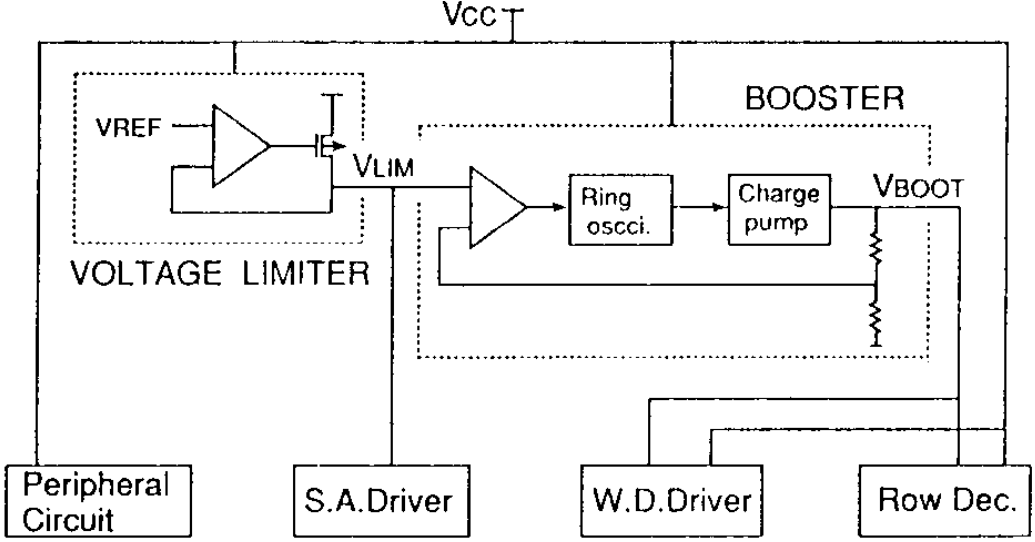
The wordlines in memory chips present heavy capacitive loads to the address decoders, and thus specialwordline driver circuits are needed to drive these lines. Employing a smaller array will improve the performance; however, the overhead of WL drivers (WLDVs), column decoders (CDECs), and the sense amplifiers (SAs) will also be increased [1]. The term sense amplifier refers to a collection of circuit elements that pitch up to the digitlines of a DRAM array. This collection most generally includes isolation transistors, devices for digitlines equilibration and bias, one or more Nsense-amplifiers, one or more Psense-amplifiers, and devices connecting selected digitlines to I/O signal lines. All of the circuits along with the worldline driver circuits are called pitch cells. [2] Figure 4979a shows that main-word-lines (MWL0, MWL0B) driven by row decoders is laid out in a two or four times pitch as sub-word-lines. The row decoder and the word-drive decoder include CMOS output gates for the stable operation of main and sub word-lines. Boosted voltage (VBOOT) is supplied to not only word drive decoders but also row decoders to charge the gate of the sub-word-drive-transistor enough to realize the fast decoding even with the small sub-word-drive-transistor. By integrating the decoding circuit and the voltage converter to transform the lower voltage signals into the boosted voltage level. Only the output gate of the word-reset signal-line (MWLOB) is driven at the external voltage (VCC) instead of VBOOT for reduction of the power dissipation.
Figure 4979b shows the schematics of a typical power supply of DRAM. There are three voltage levels:
As shown in Figures 4979c, a typical local wordline driver stripe has 3 transistors per local wordline. The share of local wordline driver area is between 5% and 10%.
[1] T. Kimuta, K. Takeda, Y. Aimoto, N. Nakamura, T. Iwasaki, Y. Nakazawa, H. Toyoshima,
M. Hamada, M. Togo, H. Nobusawa, T. Tanigawa, 64 Mb 6.8 ns random ROW access DRAM
macro for ASICs, ISSCC, Dig. Tech. Papers, Feb 1999, pp. 416–417.
|
||||||||
| ================================================================================= | ||||||||
|
|
||||||||