|
|||||||||||||||||||||||||||||||||||||||||||||||||
Sense Amplifier (SA, S/A) in DRAM
- Integrated Circuits and Materials - - An Online Book - |
|||||||||||||||||||||||||||||||||||||||||||||||||
| Integrated Circuits and Materials http://www.globalsino.com/ICsAndMaterials/ | |||||||||||||||||||||||||||||||||||||||||||||||||
| ================================================================================= | |||||||||||||||||||||||||||||||||||||||||||||||||
During a read operation in memory chips, the signal coming from the cell can be quite small, and sense amplifiers are required to detect the state of the memory cell and restore the signal to a full logic level for use in the external interface. The term sense amplifier refers to a collection of circuit elements that pitch up to the digitlines of a DRAM array. This collection most generally includes isolation transistors, devices for digitlines equilibration and bias, one or more Nsense-amplifiers, one or more Psense-amplifiers, and devices connecting selected digitlines to I/O signal lines. All of the circuits along with the worldline driver circuits are called pitch cells. [4] Variation in the capacitance of individual cells in DRAM is presumably tolerated by the operating window of the sense amplifiers. [16] The read process of all memory devices is common. After settling the predefined voltage to the bit line, the bit line is electrically connected with the memory cell. Then, the stored bit information of the cell will modulate the bit line voltage or current. The modulated analog value (voltage or current) of a bit line is then converted to the digital value (namely, GND or VDD) by the sense amplifier (SA) circuit.
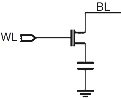
Figure 4989a. DRAM and its equivalent circuit models. [1]
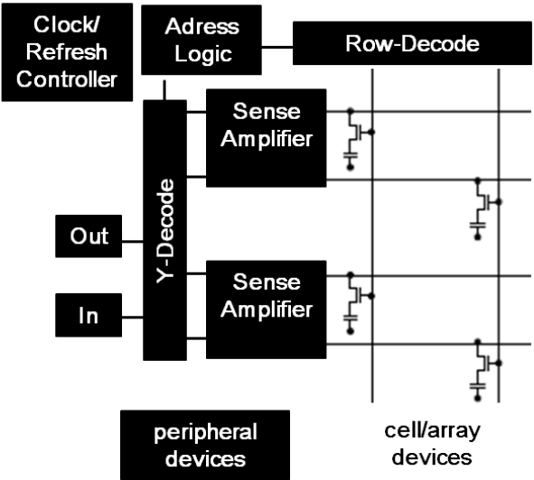
Figure 4989b. Structure of DRAM and peripheral circuitry. [14]
Figure 4989c. Peripheral DRAM circuitry and the array devices. [15] Figure 4989d shows two examples of sense amplifiers. The selection criterion of sense amplifiers is determined by the circuit area and operating speed.
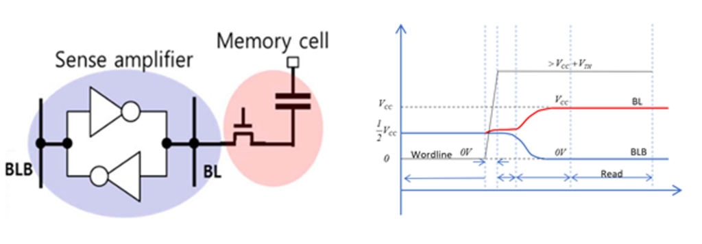
By combining the circuits in Figure 4989a and 4989d, the circuit in Figure 4989e can be obtained for DRAM with a voltage SA.
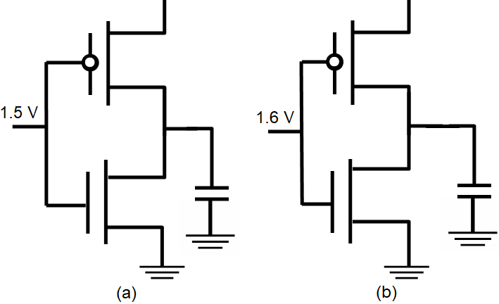
Latch in a SA will be working as the logic circuit not the analog circuit, so that its operation is very robust to the process variations. Since many numbers of a SA will bring the large leakage current, then it is necessary to control some device parameters related to the threshold voltage such as doping density, channel length and width, etc. When inputs at different voltages are applied to the CMOS invertors shown in Figure 4989f, then the inverter in Figure 4989f (b) will discharge the output capacitor faster because ID is proportional to VGS. In other words, the output in Figure 4989f (b) will reach logic zero faster.
In an inverter, e.g. SA, the PMOS is connected to VDD and the NMOS is connected to ground (GND). The gate terminals of both NMOS and PMOS are connected together and act as the input terminal (see Figures 4989g and 4989h). The drains of both are tied together and act as the output terminal. The inverter has only two states. There is never a short circuit between VDD and ground when the inverter is in a stable state, that is, when the output is either logic high or logic low. Therefore, in the steady state power dissipation is negligible because no current flows from VDD to ground as when one transistor is on and the other is off. The only time current flows from VDD to ground is for a very short duration when the output switches from one state to the next. During this very short interval when one transistor is going from off to on and the other is going from on to off. A short current spike flows during this transition and this is the only time power is dissipated in the inverter. Table 4989 shows that CMOS is used because such digital circuits have the lowest power consumption. Table 4989. Power consumption in an inverter, NMOS and PMOS.
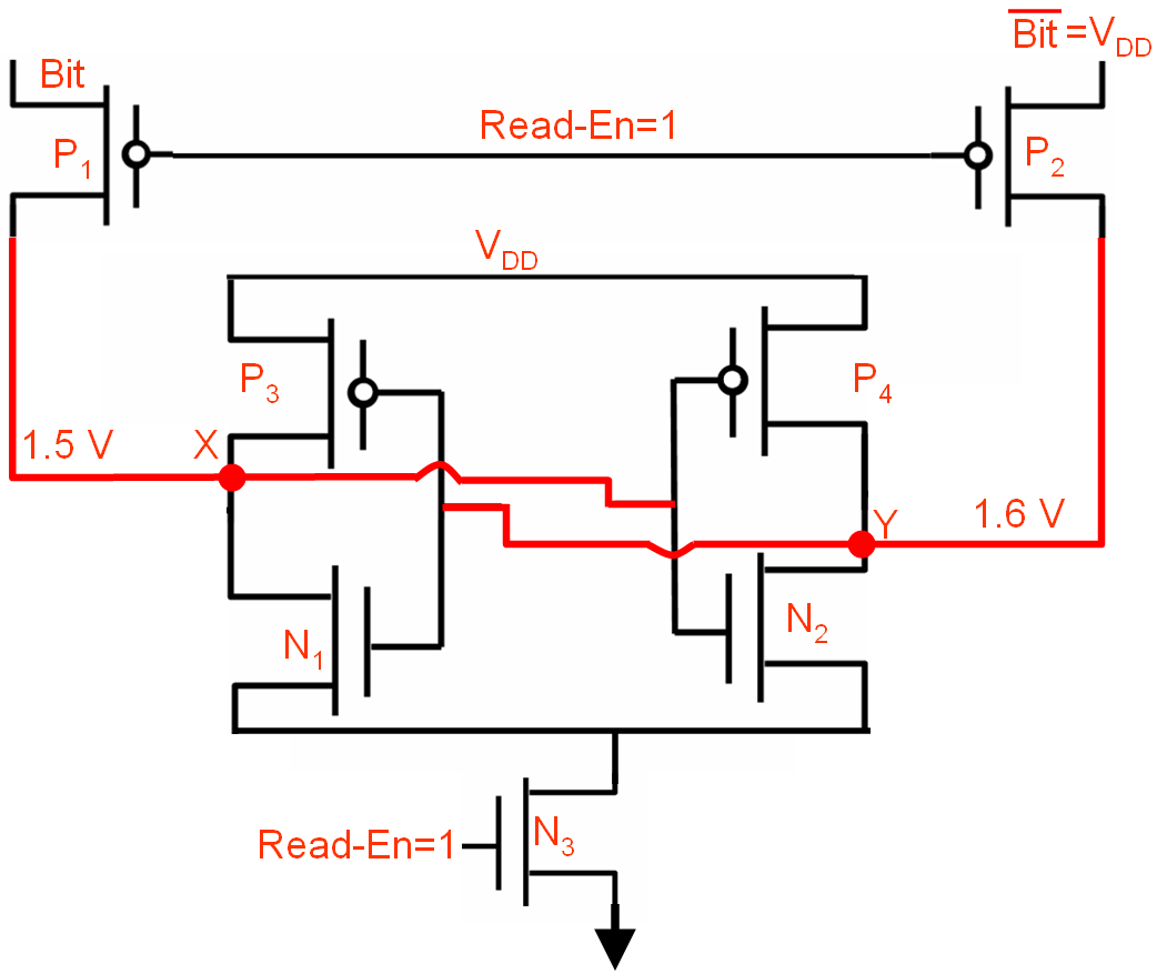
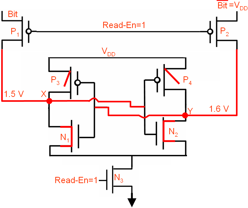
An example of application of a SA is shown in Figures 4989g and 4989h. Assuming two voltages (1.5 V and 1.6 V) with a small difference of 0.1 V are applied to nodes X and Y in Figures 4989g. Then, we can see the process below (as shown in Figures 4989h): SA senses the voltage difference between the two bit lines and amplifies it. Therefore, although noise will be included in the process, but since SA detects the voltage difference, it doesn't matter if BL and BLB include the same amount of noise and the same amount of voltage fluctuation.
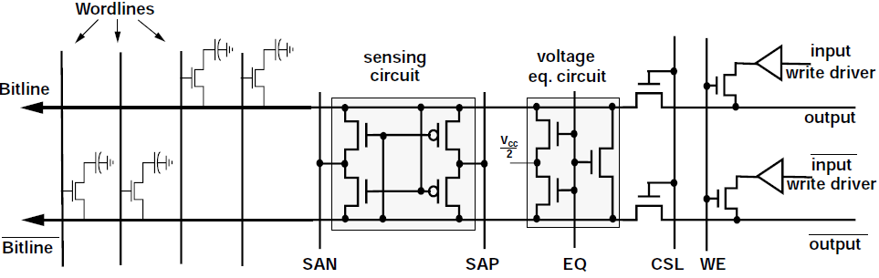
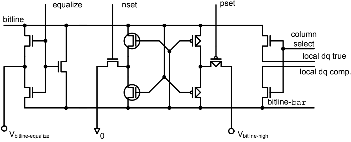
Employing a smaller array will improve the performance; however, the overhead of WL drivers (WLDVs), column decoders (CDECs), and the sense amplifiers (SAs) will also be increased [2]. Figure 4989i shows a diagram of a basic sense amplifier. More complex sense amplifiers in modern DRAM devices contain:
Figure 4989i. Diagram of a basic sense amplifier. [5]
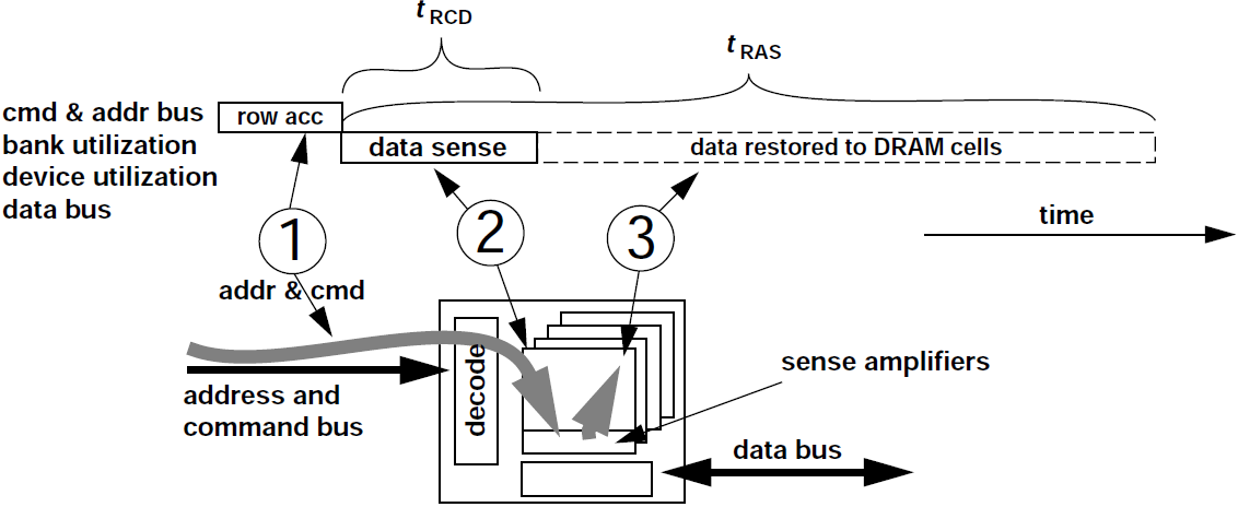
Figure 4989j. Row access command and timing. [5]
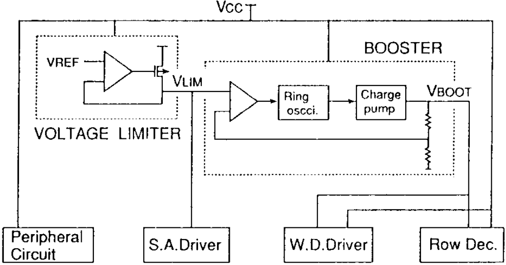
Figure 4989k. Row precharge command and timing. [5] Figure 4989l shows the schematics of a typical power supply of DRAM. There are three voltage levels:
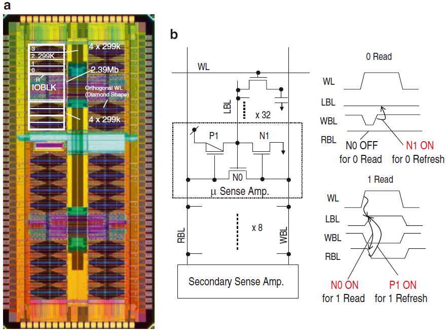
2.39 Mb embedded DRAM (eDRAM) macros [3] shown in Figure 4989m are organized by upper and lower memory units, each consisting of four 299 Kb sub-arrays (0 through 3) and a 16 row redundancy array (R). They are supported by the Input and Output circuitry (IOBLK) located between two memory units. When the macro decoder receives a valid macro-select-signal and a valid read or write command, then the decoder evaluates the address, activating either the top or bottom memory units. The activation of the memory unit enables one of the four arrays, and sends 1 of 256 valid addresses. The 299 Kb sub-array includes ECC bits for IBM servers. An evolutionary approach in this eDRAM locates the segmented WL drivers in the sense amplifier area, which couples to the horizontally arranged WLs through the vertically arranged wires.
Figure 4989n shows that main-word-lines (MWL0, MWL0B) driven by row decoders is laid out in a two or four times pitch as sub-word-lines. The row decoder and the word-drive decoder include CMOS output gates for the stable operation of main and sub word-lines. Boosted voltage (VBOOT) is supplied to not only word drive decoders but also row decoders to charge the gate of the sub-word-drive-transistor enough to realize the fast decoding even with the small sub-word-drive-transistor. By integrating the decoding circuit and the voltage converter to transform the lower voltage signals into the boosted voltage level. Only the output gate of the word-reset signal-line (MWLOB) is driven at the external voltage (VCC) instead of VBOOT for reduction of the power dissipation.
When reading stored data, the bit line(BL) and bit line bar(BLB) are compared: The BLB becomes a standard point because it is not connected to the cell. Because the signal difference between BL and the BLB is very small, it is amplified through the sense amplifier circuit to read data as shown in Figure 4989o.
As shown in Figures 4989p, a typical bitline sense-amplifier stripe has 11 transistors per bitline pair, a typical local wordline driver stripe has 3 transistors per local wordline. The share of bitline sense-amplifier area to total die area in a typical DRAM die is between 8% and 15%.
Figure 4989q shows the data transfer from CPU to DRAM memory in a computer.
The traditional purpose of
isolation devices in DRAMs is used to separate the active cross-coupled pair(s) from the large bitline
capacitances during initial sensing. If the bitline capacitance is very large, the isolation
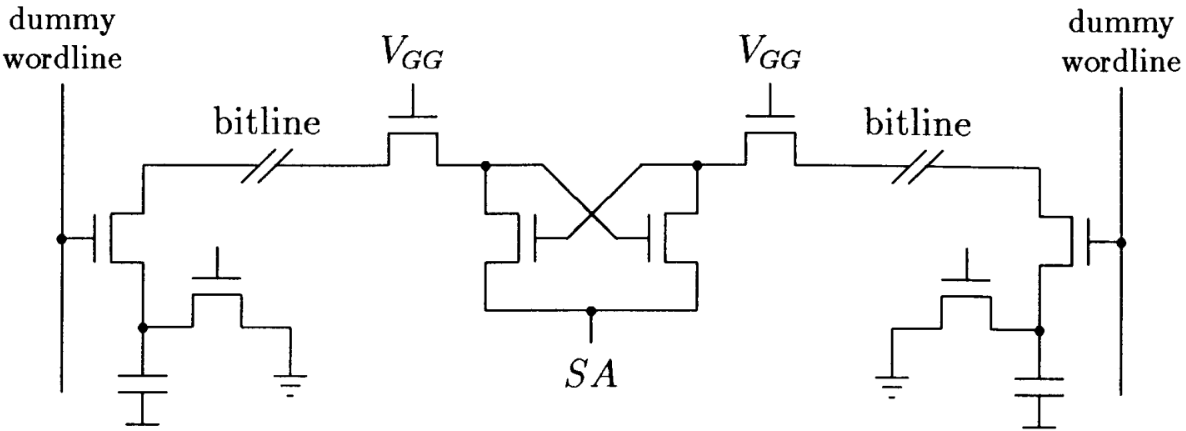
devices may significantly improve amplifier speed and sensitivity. [18] Figure 4989r shows a Mostek DRAM sense amplifier. The isolation devices are used to partially decouple the sense amplifier signal nodes from the bitline segments, with an internal 16 V supply, VGG, tied to the gates of the isolation devices. Two operations are:
Note that Gealow's thesis also presented the layouts of sense amplifiers, sense amplifier precharge circuits, sense amplifier cross-coupled pair, and isolation devices. [18] Figure 4989s shows an example of waveforms for the read-modify-write cycle
[1] Krzysztof (Kris) Iniewski, CMOS Processors and Memories, 2010.
|
|||||||||||||||||||||||||||||||||||||||||||||||||
| ================================================================================= | |||||||||||||||||||||||||||||||||||||||||||||||||
|
|
|||||||||||||||||||||||||||||||||||||||||||||||||