VSS in DRAM - Integrated Circuits - - An Online Book - |
|||||||||||||||||||||||||||||||||||||||
| Integrated Circuits http://www.globalsino.com/ICsAndMaterials/ | |||||||||||||||||||||||||||||||||||||||
| ================================================================================= | |||||||||||||||||||||||||||||||||||||||
VSS refers to the ground or the negative power supply voltage. It is used as the reference point in the circuit, representing the "low" voltage level or 0 volts. VSS is the voltage applied to the source of an N-channel MOSFET or the drain of a P-channel MOSFET. The read process of all memory devices is common. After settling the predefined voltage to the bit line, the bit line is electrically connected with the memory cell. Then, the stored bit information of the cell will modulate the bit line voltage or current. The modulated analog value (voltage or current) of a bit line is then converted to the digital value (namely, GND or VDD) by the sense amplifier (SA) circuit.
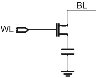
Figure 4997a. DRAM and its equivalent circuit models. [2] The MOS is polarized with a gate always on, the drain at VSS, and the source at VDD. VDD is the power supply. Table 4997a. Logic levels and their corresponding symbols in Dsch and Microwind tools.
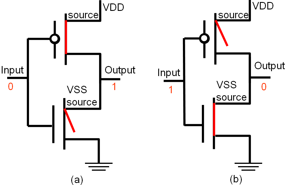
Figure 4997b. PMOS and NMOS diagrams. Table 4997b lists outputs of PMOS and NMOS inputs. Both CMOS and PMOS in circuits act as inverters. Figure 4997c shows an diagram of CMOS outputs with different inputs. When the input signal is logic 0, the nMOS is switched off while the pMOS passes VDD through the output, which turns to 1. When the input signal is logic 1, then the pMOS is switched off while the nMOS passes VSS to the output which goes back to 0. Table 4997b. Outputs of PMOS and NMOS inputs.
When a voltage is applied voltage on the word line (WL) and the transistor is turned on, the charges are stored in the capacitor through the bit line. At this time, when a high voltage(Vdd) is applied to the bit line (BL), DATA 1 is stored in the capacitor, and when a low voltage (Vss, 0 V) is applied, DATA 0 is stored.
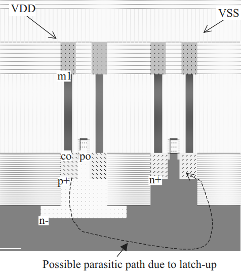
Figure 4997c. Diagram of CMOS outputs with different inputs. The latch-up effect is a parasitic shortcut between VDD and VSS, which can lead to the destruction of the integrated circuits. The origin of latch-up is the activation of a parasitic N/P/N/P device (also called thyristor) appearing in the vertical cross-section of the nMOS and pMOS structures as shown in Figure 4997d.
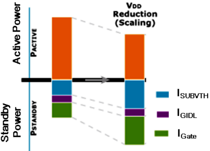
Figure 4997d. Origin of latch-up. [1] Leakage power in DRAM is proportional to VDD. Figure 4997e shows that the standby power is increased by subthreshold leakage (ISubVth), gate induced drain leakage (IGIDL), and gate leakage (IGate) through a thinner gate oxide layer.
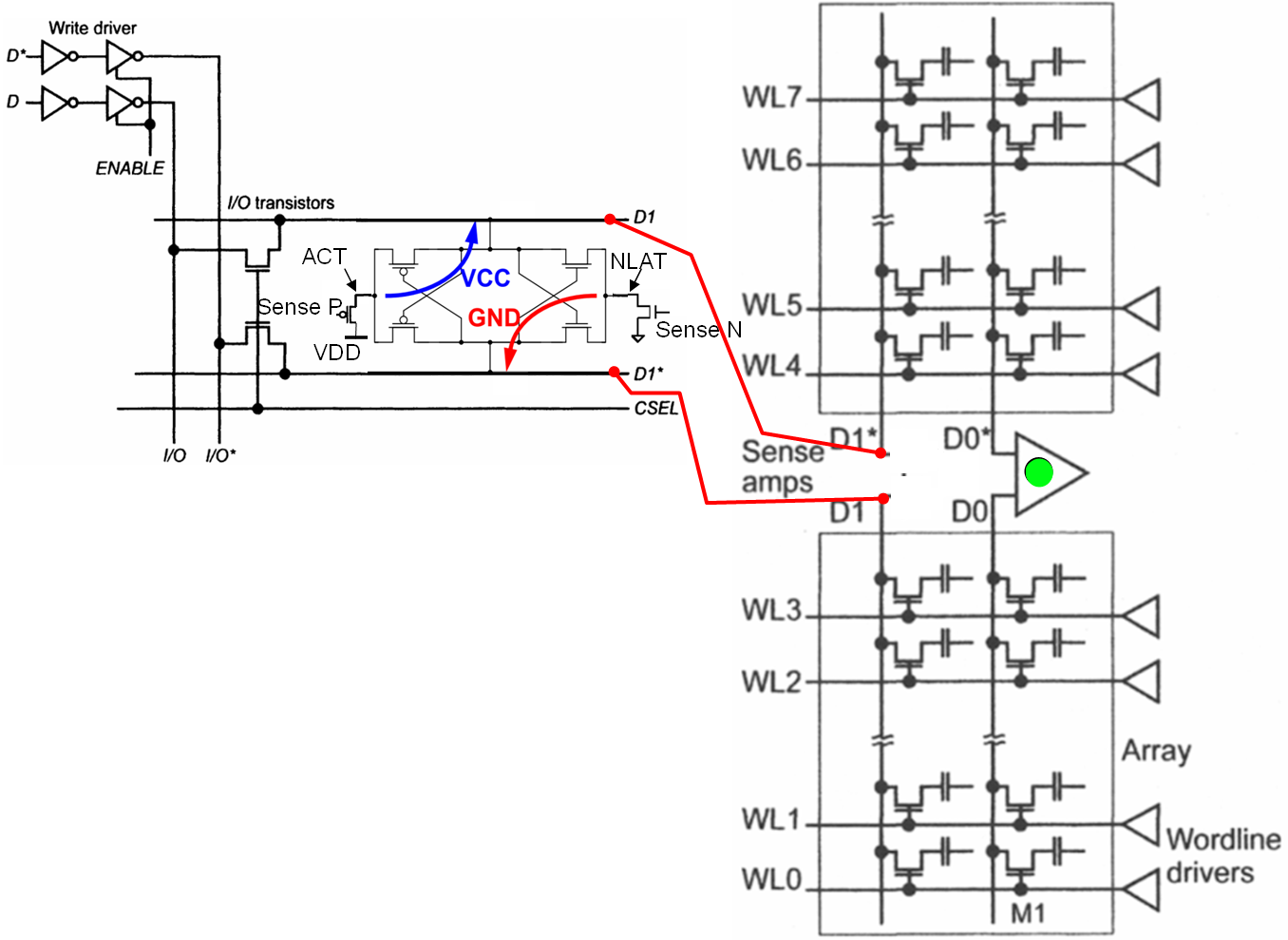
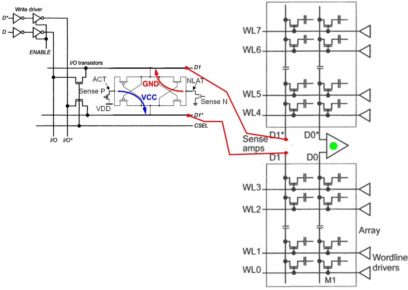
Figure 4997f shows sense amplifier schematic with I/O devices. Initially, ACT is at VSS (GND) and NLAT* held at VCC/2. while both D1 (BL1) and D1* (BL1*) are at VCC/2 as well. The start of the read operation is the node sense N, which have 0V voltage levels. When reading, the wordline is pulled to VCC+Vth and BL1/* changes. After the cell has been accessed, a sense amplifier pulls up the voltage differential between the two column lines. The sensing is essentially the amplification of the differential voltage between the two column lines D1 and D1*. The P sense amplifier and the N sense amplifier are normally fired sequentially. The NSA is first fired by bringing NLAT* (N sense-amplifier latch) toward ground. The voltage difference between NLAT and the column lines increases so that the NMOS transistor whose gate is connected to the higher voltage column line begins to conduct. Such conduction causes the low-voltage column to be brought to discharge towards NLAT* and finally to be brought to ground voltage. However, the other NMOS transistor will not conduct. In some cases, after the N sense amplifier has fired, ACT (for active pull-up) will be brought towards VCC to activate the P snese amplifiers. The low-voltage column line is close to ground so that the corresponding PMOS transistor is driven into conduction. This charges the high-voltage column line towards ACT and ultimately towards VCC. Therefore, all column lines are either driven to high or to low according to the contents of the DRAM cell in the row.
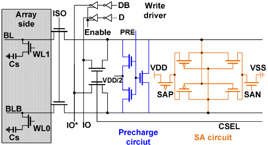
Figure 4997g shows the schematic diagram of a conventional sensing circuit and a 1T1C DRAM array. IO* means inverted signal of IO.
[1] Etienne Sicard, Basics of CMOS Cell Design, 2007.
|
|||||||||||||||||||||||||||||||||||||||
| ================================================================================= | |||||||||||||||||||||||||||||||||||||||
|
|
|||||||||||||||||||||||||||||||||||||||