|
|
EDX - Energy Dispersive X-ray Analysis
The intensity or area of a peak in an EDX spectrum is proportional to the concentration of the corresponding element in the specimen. For determining elemental content, the electron-beam current is assumed to be uniform throughout the specimen and electron channeling is avoided by avoiding strong diffraction conditions. Energy Dispersive X-ray Analysis (EDX) technique is used for performing chemical analysis in conjunction with Scanning Electron Microscopy (SEM) and Transmission Electron Microscopy (TEM) and is not a surface science technique. The analytical data are acquired in the form of digitised spectra, viewed during accumulation on a computer monitor, which display the number of x-rays, I, detected as a funciton of E, the x-ray energy. An electron beam strikes the surface of a conducting sample (SEM) or of a thin film (TEM). The energy of the beam is typically in the range of 10-20 keV. This causes X-rays to be emitted from the irradiated material. The energy of the X-rays emitted depend on the material under examination. The X-rays are generated in a region about 2 microns in depth (SEM), and thus EDX is not a surface science technique. By moving the electron beam across the material an 2-D (two dimensional) image of each element in the sample can be acquired. Due to the low X-ray intensity, images usually take a number of hours to be acquired. Elements of low atomic number are difficult to detect by EDX. A Beryllium window is often used to protect the SiLi detector in the EDX system. The absorbtion of the soft X-rays by the Be precludes the detection of elements below an atomic number of 11 (Na). In windowless EDX systems, elements with as low atomic number as 4 (Be) have been detected, but the problems involved get progressively worse as the atomic number is reduced. Morever, an absorption correction of transmission EDX spectra (TEM) requires parameters such as specimen thickness, X-ray take-off angle, and specimen density. Spatial resolution of X-ray microanalysis in the (S)TEM is limited by the initial electron probe size and by subsequent beam broadening in the film. The Lithium drifted Silicon (SiLi) detector The x-ray detector design is influenced by limited access to the sample due to the proximity of the objective lens pole-pieces, aperture rod, anti-contamination devices, and the sample holder. Hence, the solid-state energy-dispersive (semiconductor) detector is preferred to crystal spectrometers and propertional counters. Although, Ge detectors were developed first, for high-energy radiation analysis, the Si detector was more efficient for analysis of the low energy x-rays generated in electron microscopes. The detector used in EDX is often the Lithium drifted Silicon detector. This detector must be operated at liquid nitrogen temperatures. When an X-ray strikes the detector, it will generate a photoelectron within the body of the Si. As this photoelectron travels through the Si, it generates electron-hole pairs. The electrons and holes are attracted to opposite ends of the detector with the aid of a strong electric field. The size of the current pulse thus generated depends on the number of electron-hole pairs created, which in turn depends on the energy of the incoming X-ray. Thus, an X-ray spectrum can be acquired giving information on the elemental composition of the material under examination.
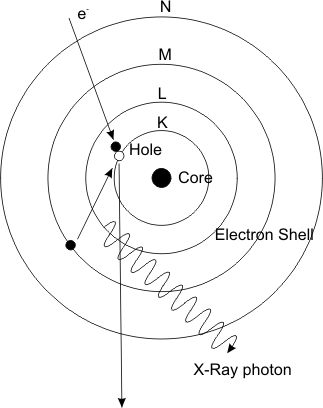
Scheme of X-Ray excitations
An inner shell electron is ejected (e.g. K shell)--This is the primary event which leads to a characteristic loss of energy by the incident electron that is the basis for EELS. This electron is replaced by an electron from higher energy shell (e.g. L) Detection -- X-rays are emitted over all possible angles ==> detectors must be placed as close as possible in order to collect the maximum number of emitted X-rays. 1. Wavelength Dispersive Spectrometer -- Disperse X-rays using a crystal monochromater. As in a UV/Vis spectrophotometer, one can select a single wavelength to measure by positioning a slit which only lets a narrow band of wavelengths pass. Provides very high resolution (ca. 10 eV) but is very inefficient. 2. Energy Dispersive Detector (EDS) -- Emitted X-rays strike a solid state detector producing a transient electrical signal who's energy is proportional to the energy of the X-ray. These signals are sorted according to their energy and counted in a multichannel analyzer. The energy resolution is only 150-200 eV. The spatial resolution of EDS is approximately 1 μm for SEM imaging and down to 10 nm for TEM imaging. EDS identifies elements with a relative concentration of 0.1% or higher. It is different from EELS measurements, EDS is more accurate for heavy elements and less accurate for light elements. Contact the author: Feedback
|
|
||||||||
|
Copyright (C) 2006 GlobalSino, All Rights Reserved
|