ADF(HAADF)-STEM Contrast at Interfaces - Practical Electron Microscopy and Database - - An Online Book - |
|||||||||||||||||||||||||||||||||||||||||
| Microanalysis | EM Book http://www.globalsino.com/EM/ | |||||||||||||||||||||||||||||||||||||||||
| ================================================================================= | |||||||||||||||||||||||||||||||||||||||||
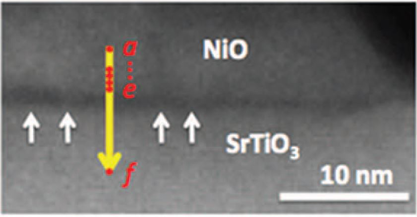
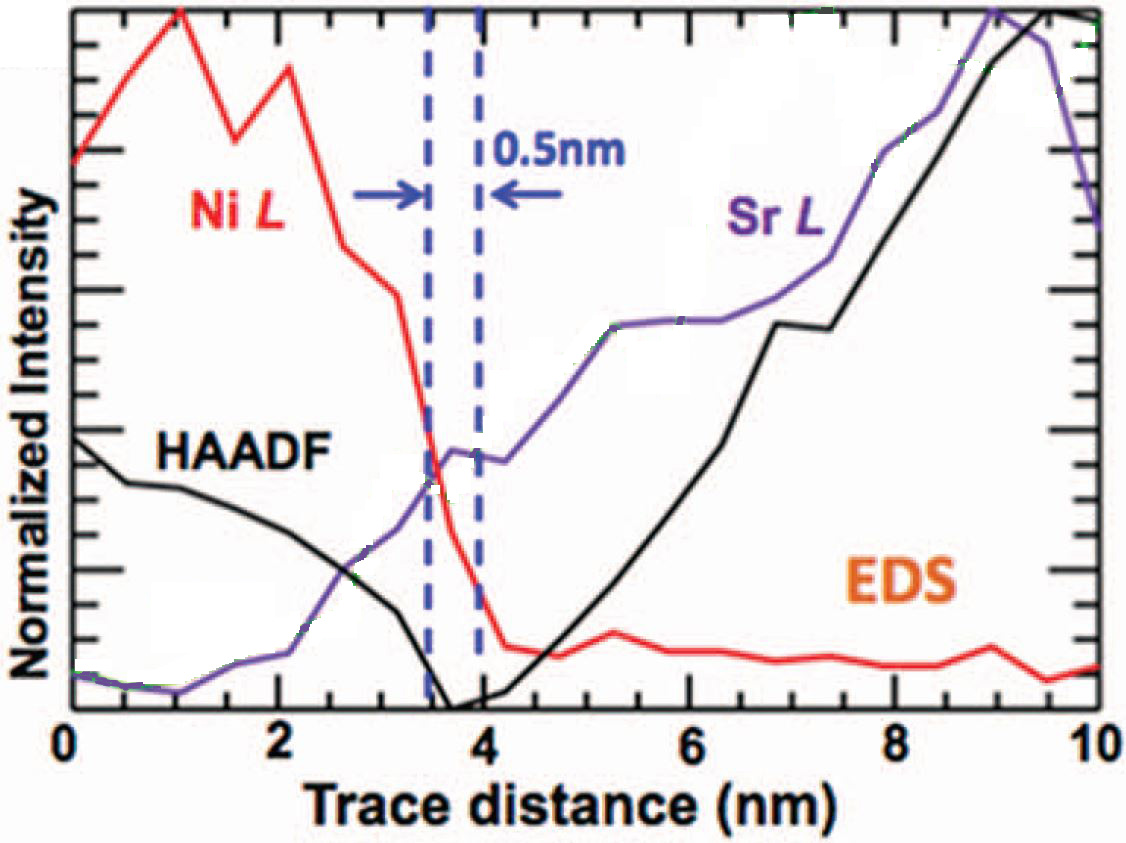
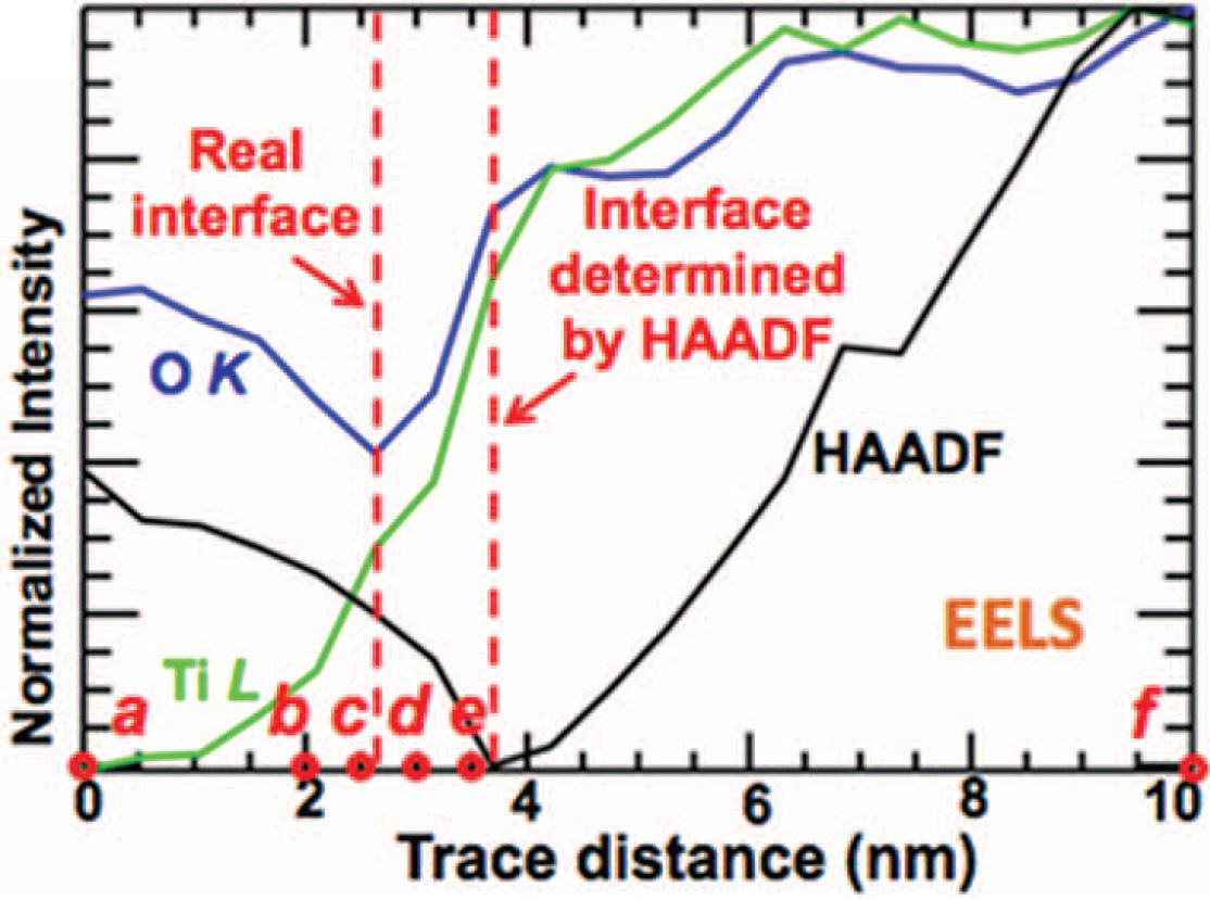
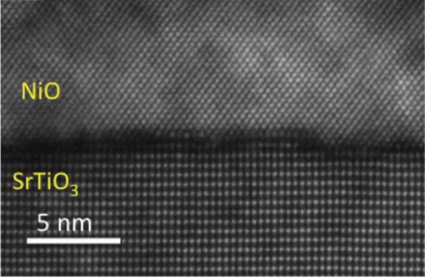
HAADF-STEM Contrast at Interface between Two Crystals In most cases, the interface between two crystals is not ideal. It is very common that the atomic number of the interface is lower than those of the crystalline bulks and there is chemical intermixing between them. For instance, nickel oxide (NiO) nanocrystals epitaxially grown on (001) strontium titanate (SrTiO3) single crystal substrates [1] had been characterized by aberration corrected high angle annular dark field scanning transmission electron microscopy (HAADF-STEM). The rough and irregular interface between the NiO and SrTiO3 crystals had a lower average atomic number than the two crystalline bulks as indicated by the dark layer at the interface shown in Figure 1352 (a) and (d). Figures 1352 (b) and (c) show EDS (for Ni and Sr) and EELS (for O and Ti) data, respectively, simultaneously acquired from a line scan across the NiO-SrTiO3 interface (marked as a yellow arrow in Figure 1352 (a)). Figure 1352 (c) suggests lack of a sharp interface in the O K profile and presence of oxygen vacancies at the NiO-SrTiO3 interface. Figures 1352 (b) and (c) show that there is intermixing between NiO and SrTiO3 near the interface. Figure 1352 (c) shows that the real interface, where the oxygen minimum locates, is not the same as the interface, represented by the minimum of HAADF contrast.
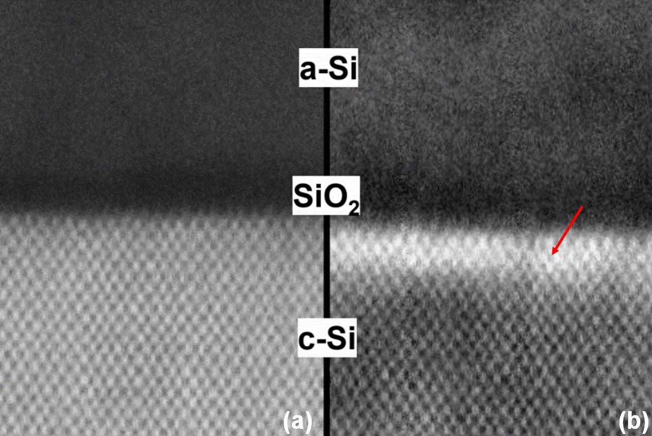
HAADF-STEM Contrast at Interface between Amorphous and Crystalline Layers Table 1352a lists the possible contrast mechanisms of bright-band in the Si (silicon) crystal at an a-SiO2/c-Si interface or an a-Si/c-Si interface in an ADF-STEM image. Table 1352a. Possible contrast mechanisms of bright-band of c-Si at a-Si or a-SiO2/c-Si interfaces.
Other factors such as sample thickness effect in zone-axis crystals [7] and detector inner angle, as shown in Table 1352b, may also affect the appearance of strain contrast in ADF images. In the existing of strain fields, the scattering of electrons results in different angular distributions and thus the intensity collected by the ADF detector from the strained region can be different than that from the strain-free region, resulting in strain contrast. The thickness dependence of strain contrast originates from the propagation process of the electron beam with the channeling effect [8-11] inside a zone-axis crystal.
As shown in Figure 1352, when the strain amplitude increases, the channeling effect decreases, which is also called dechanneling. Therefore, the strain fields cause dechanneling.
|
|||||||||||||||||||||||||||||||||||||||||
| ================================================================================= | |||||||||||||||||||||||||||||||||||||||||
|
|
|||||||||||||||||||||||||||||||||||||||||