EDS Measurement of Tantalum (Ta) - Practical Electron Microscopy and Database - - An Online Book - |
||||||||
| Microanalysis | EM Book http://www.globalsino.com/EM/ | ||||||||
Figure 1403a shows a deconvoluted X-ray spectrum taken from a material containing Ta, Sr, Zr, Nb, and Pb elements. The different colored peaks represent the contribution of the various elements. The grey area is the background corrected spectrum which is the sum of all the deconvoluted lines.
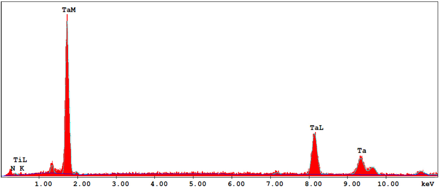
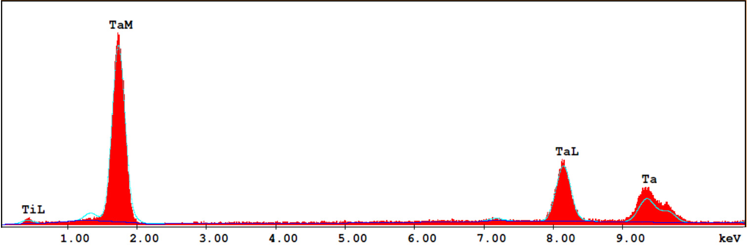
Figures 1403b and 1403c show EDS spectra of 5 μm and 12 μm thick Ta films deposited on Si substrates with nitrogen flow rates of 5% and 0%, respectively [2]. The spectra were taken in a same SEM system. No Si signal was detected so that the interaction volume is shallower than the Ta thicknesses. We can see that the ratios of M and L peak heights in the two figures are different most likely due to the Ti impurity in the Ta films.
[1] T. Salge, R. Neumann, C. Andersson, M. Patzschke, Advanced Mineral Classification Using Feature Analysis and
Spectrum Imaging with EDS, 23rd International Mining Congress & Exhibition of Turkey, 16-19 April, 357, 2013.
|
|
|||||||