=================================================================================
Based on band theory, when a large number of atoms combine to form a large aggregate, molecular orbitals merge into an almost continuous band of energy levels. The bottom half (called valence band) of the band is composed of bonding M.O.s (molecular orbitals) and is filled with electrons. The upper half (called conduction band) of band is composed of antibonding M.O.s and is empty.
In general, those electrons in different orbitals form their own energy levels of valence and conduction bands as shown in Figure 2633a.
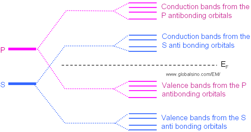
Figure 2633a. Schematic illustration of evolution of the atomic s and p orbitals into valence and conduction bands in some materials.
For instance, the schematic illustration in Figure 2633b shows the bonding levels for diamond and indicates the formation of valence band. When the hybrid carbon atoms bond, a second electron is contributed to the state by the other atom, and thus the interaction between the two electrons lowers the energy of the state. Therefore, the sp3 energy level splits into a series of four bonding and four antibonding orbitals. In an actual solid, there is a Coulomb interaction between the atom cores and the electrons, and then the bonding and anti-bonding energy levels split to form a continuous band structure, with the band of bonding states being the valence band and the anti-bonding states being the conduction band.
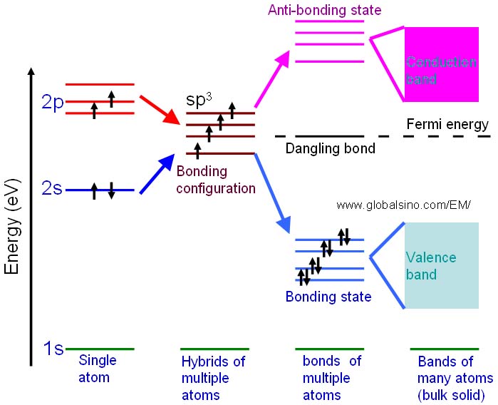
Figure 2633b. Schematic illustration showing the progression of the electronic structure for an sp3 bonded system.
The valence band electrons normally originate from the electrons in the incomplete outer shell of atoms, for instance, the valence band is formed for silicon (Si) crystals as shown in Figure 2633c. An isolated Si atom contains 14 electrons, which occupy 1s, 2s, 2p, 3s and 3p orbital in pairs. When atoms are far away from each other, the electrons in the out shell do not interact. As the distance between atoms is reduced to d1, there is an overlap of electron wavefunctions across adjacent atoms. This leads to a splitting of the energy levels consistent with Pauli exclusion principle, and forming energy bands. This splitting leads to 2N states in the 3s band and 6N states in the 3p band, where N is the number of Si atoms in the crystal. A further reduction of the lattice spacing causes the 3s and 3p energy bands to merge into a single band having 8N available states, and then split again into two bands containing 4N states each. At the temperature of zero Kelvin, the lower band is completely filled with electrons and named as the valence band. The upper band is empty and named as the conduction band. Note that in crystal Si (with lattice spacing d0), the core level electrons do not start yet to interact.
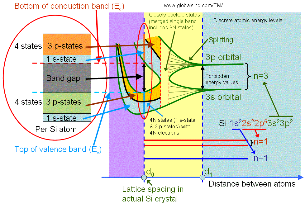
Figure 2633c. Detailed illustration of electronic structure of silicon as a function of distance between atoms. The left red circle is a zoom-in of the right red circle.
Those valence-band electrons are the only electrons:
i) Will combine with the electrons of other atoms to form compounds.
ii) Cause electric current to flow. For the same reason, the outer electrons of the atoms of a conductor are also called free electrons.
Figure 2633d shows the schematic illustration of the energy level diagrams for molecular structures with different number of atoms which are single atoms, dimers, clusters and bulk materials. Splitting of the atomic energy levels occurs when the single atoms form a diatomic molecule. As more atoms join the system, the levels split further until a quasi-continuous band structure is formed in the bulk material. In other words, quantum size effects occur when the quasi-continuous band structure of a solid state system begins to break down as more atoms are included.
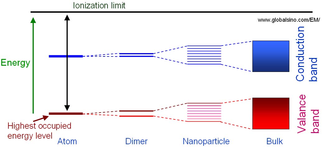
Figure 2633d. Schematic illustration of the energy level diagrams for molecular structures with different number of atoms which are single atoms, dimers, clusters and bulk materials.
The gap between the top of valence band and the bottom of conduction band is defined as energy gap Eg. In insulators, the energy gap is very large and no vacant conduction band is available to the valence electrons. Otherwise, the energy gap is either zero due overlapping between valence and conduction bands for metals or is very small for semi-conductors so that conduction band is easily available to valence electrons.
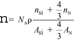
For instance, the density (n) of valence electrons in Si3N4 is given by,
 ------------------------- [2633] ------------------------- [2633]
where,
ρ -- The Si3N4 atomic density,
NA -- The Avogadro number,
ASi and AN -- The atomic weights of silicon and nitrogen, respectively,
nSi and nN -- The numbers of valence electrons per silicon and per
nitrogen atom taking part in the plasmon oscillation, respectively.
The sp2 bonded solids have both σ/σ* and π/π* states available to the electrons, while for sp3 bonded solids only the σ/ σ* states present. For the diamond and graphite, electron transitions to these states generate many of the characteristic features in EEL spectra. For instance, in core loss spectra from diamond, the excitation of the 1s electrons to the σ* states generates the carbon k edge peak. For graphite, the transitions of the inner shell electrons into unoccupied π* states give a peak prior to the edge onset. In the valence band, valence electron transitions into the π* states also produce a peak at around 6 eV.
As shown in Table 2633, the outermost shells are relatively loosely bound to the atomic nucleus.
They may absorb a small amount of energy from incident electrons and then jump to an excited state. These
energies are typically below some tens of electron volts (eV).
Table 2633. Outermost atomic electrons in various materials.
Materials |
Outermost atomic electrons |
Metallic species |
Loosely bound electrons (free-electron gas, or called electrons in conduction-band) |
|