=================================================================================
It is better to use the k factors with Fe as the standard, namely kAFe, instead of kASi, for elemental evaluations because of two reasons. Firstly, the error of the detected Si x-ray intensity, due to Si Kα absorption in the specimen, is larger than that of Fe Kα. Secondly, the EDS detector is almost 100% efficient for the detection of Fe Kα X-ray, while for Si Kα x-ray the detection efficiency is significantly degraded due to x-ray absorption in the detector itself.
Figure 3778a shows the comparison between EDS and WDS for WSix alloy. The EDS spectrum in red shows a single peak with a Full-Width Half-Maximum (FWHM) of 260 eV, while the WDS with higher energy resolution in green reveals the presence of both tungsten and silicon (FWHM: < 40 eV).
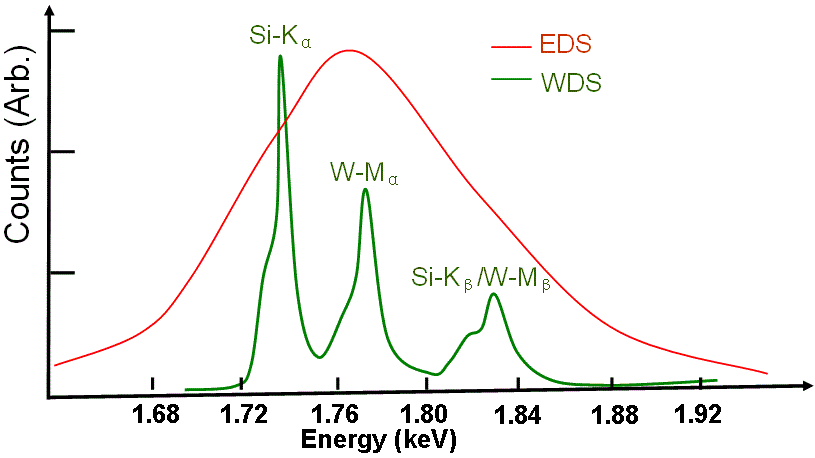
Figure 3778a. Comparison between EDS and WDS for WSix alloy.
As discussed on page4650, X-ray absorption is a function of the energy of X-rays. Low energy peaks will be more strongly absorbed than high energies ones. For thick TEM samples, k-factor correction due to X-ray absorption is needed in order to accurately quantify EDS measurements. Table 3778 lists Si-examples of thicknesses at which the thin-film approximation is no longer valid due to X-ray absorption effects in specific materials.
| Table 3778. Examples of limits to the thin-film approximation caused by X-ray absorption: Maximum thicknesses of thin specimens for
which the absorption correction (or error) is less than ±10% and ±3%. |
Material |
10% error in kAB |
3% error in kAB |
Absorbed X-ray lines |
Primary X-ray lines |
Thickness (nm) |
SiO2 |
167 |
14 |
Si Kα and O Kα |
Si Kα (1.739 keV) and O Kα (0.525 keV) |
Si3N4 |
413 |
6 |
Si Kα and N Kα |
Si Kα (1.739 keV) and N Kα (0.392 keV) |
SiC |
13 |
3 |
Si Kα and C Kα |
Si Kα (1.739 keV) and C Kα (0.277 keV) |
Figure 3778b shows the percentage of x-ray transmitted through an H2O-ice contamination layer depending on the thickness of the H2O-ice layer up to 1 μm. As expected, the absorption effect of ice layer is greatest for the low-energy boron x-rays and the least for the silicon signal. Such H2O-ice layer is normally formed in cryo-TEM measurements.
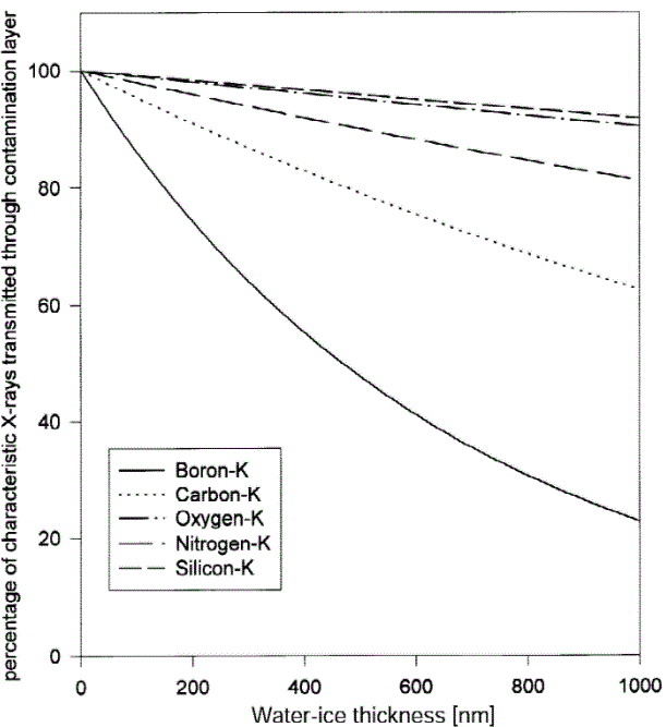
| Figure 3778b. Calculated percentage absorption of characteristic x-
rays in an H2O-ice contamination layer. [1]. X-ray energies: B-K = 183 eV, C-K = 277 eV, O-K = 525 eV, N-K = 392 eV and Si-K = 1.739 keV. |
[1] M. Malac and R.F. Egerton, Calibration Specimens for Determining Energy-Dispersive X-ray k-Factors of Boron, Nitrogen, Oxygen, and Fluorine, Microsc. Microanal. 5, 29–38, (1999).
|