=================================================================================
The sample thickness influences the spatial resolution of EM techniques. The degree of the dependence varies from technique to technique, for instance, this dependence is significant for the EDS method in EM, while the dependence is weak for AES method because AES is a surface analysis technique.
As we know that in TEM observation, the transmission of unscattered incident electrons is inversely proportional to the TEM specimen thickness. On the other hand, the increase of the specimen thickness enhances the energy loss of the transmitted electrons. Therefore, the spatial resolution degrades with the increase of specimen thickness because of the chromatic aberration effects. Table 3783 lists examples of the energy loss of incident electrons passing through the specimen. The use of thinner specimen can generally improve spatial resolution because it minimizes the energy loss.
Table 3783. Examples of the energy loss of electrons passing through the TEM specimen.
| |
Accelerating voltage of incident electrons |
Penetrated electrons (%) |
Penetrated electron with energy loss higher than 50 eV (%) |
Unscattered electrons (%) |
Elastically scattered electrons (%) |
| Thin metal foil |
|
50 |
40 |
|
|
| 50 nm thick carbon film |
50 kV |
|
55 |
33 |
10 |
If the TEM specimen is very thick, both the chromatic and spherical aberrations affect the spatial resolution of EFTEM imaging significantly. For instance, for thick specimen the chromatic broadening (Δdc) is about 2.5 nm at β = 10 mrad, Cc = 1 mm, ΔE = 50 eV, and E0 = 200 keV, while for thin specimen, Δdc will be normally ≤ 0.2 nm for most microscope configurations (see details in page3384). For thick specimen, assuming the spherical aberration constant is 0.7 mm, collection semi-angle 15 mrad, the ΔdS will be ~3.8 nm, while for thin specimen ΔdS is normally negligible for most microscope configurations (see details in page1941).
The spatial resolution of the measurements in STEM mode can be estimated by the diameter of the probe irradiation on the specimen. Assuming the thickness of the specimen is t, then the spatial resolution is given by (see Figure 3783a):
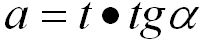 -------------------------------- [3783] -------------------------------- [3783]
where,
α -- The convergence semiangle.
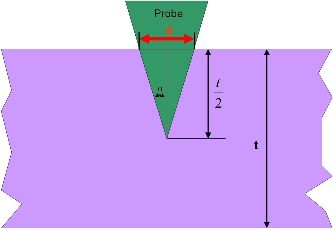
Figure 3783a. Diameter of the probe irradiation with specimen thickness t. |
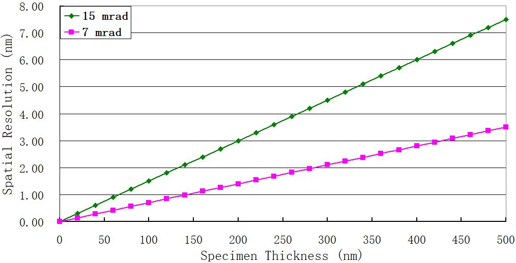
For instance, Figure 3783b shows the spatial resolutions at convergence semiangles 7 and 15 mrad, respectively, based on Equation 3783. Note that such convergence semiangles are used in many TEM systems. Therefore, in the case of a thick sample, the resolution is limited
by the probe broadening of the focused beam. [1]
| Figure 3783b. Spatial resolutions at convergence semiangles 7 and 15 mrad, respectively, based on Equation 3783. |
[1] Chuvilin A, Kaiser U, On the peculiarities of CBED pattern formation revealed bymultislice simulation. Ultramicroscopy 104:73–82, (2005).
|