Chapter/Index: Introduction | A |
B |
C |
D |
E |
F |
G |
H |
I |
J |
K |
L |
M |
N |
O |
P |
Q |
R |
S |
T |
U |
V |
W |
X |
Y |
Z |
Appendix
Intraband Transition
| An intraband transition is a transition between electronic states within the same band (intra- is a Latin word meaning ‘within’ ). For instance, there is a filled d band below the Fermi energy in noble metals used in plasmonics, and a partially filled s band where the Fermi energy is located.
Different from interband transitions, intraband transitions are an unavoidable consequence of coupling light to free carriers and are modelled by a loss parameter in the Drude function.
Figure 953 shows radiative transition processes in silicon devices. The processes can be
classified into three groups:
i) interband transitions.
i.a) intrinsic emission
with energy close to bandgap energy as shown by "1a".
i.b) high energy
transitions which involve a hot electron as shown by "1b".
i.c) high energy
transitions which involve a hot
hole as shown by "1c".
In the case of silicon (Si), it is an indirect-gap semiconductor,
interband transitions at room temperature is assisted by a
phonon emission process. The radiative emission band at
room temperature is relatively broad at energies around the
Si bandgap energy (1.12 eV) or Si bandgap
wavelength (1107 nm).
ii) deep level transitions involving chemical impurities, physical defects or
deep traps which include transitions:
ii.a) from conduction band to
acceptor level as shown by "2a".
ii.b) from donor level to valence band as shown by "2b".
ii.c) from donor
level to acceptor level as shown by "2c".
ii.d) from conduction band to deep trap level
as shown by "2d".
ii.e) from deep trap level to valence band as shown by "2e".
In these transition cases, the radiative
emission energies would generally be below the Si
bandgap energy or at wavelengths that are above the
silicon bandgap wavelength.
iii) intraband transitions involving:
iii.a) hot electrons as shown by "3a".
iii.b) hot
holes as shown by "3b".
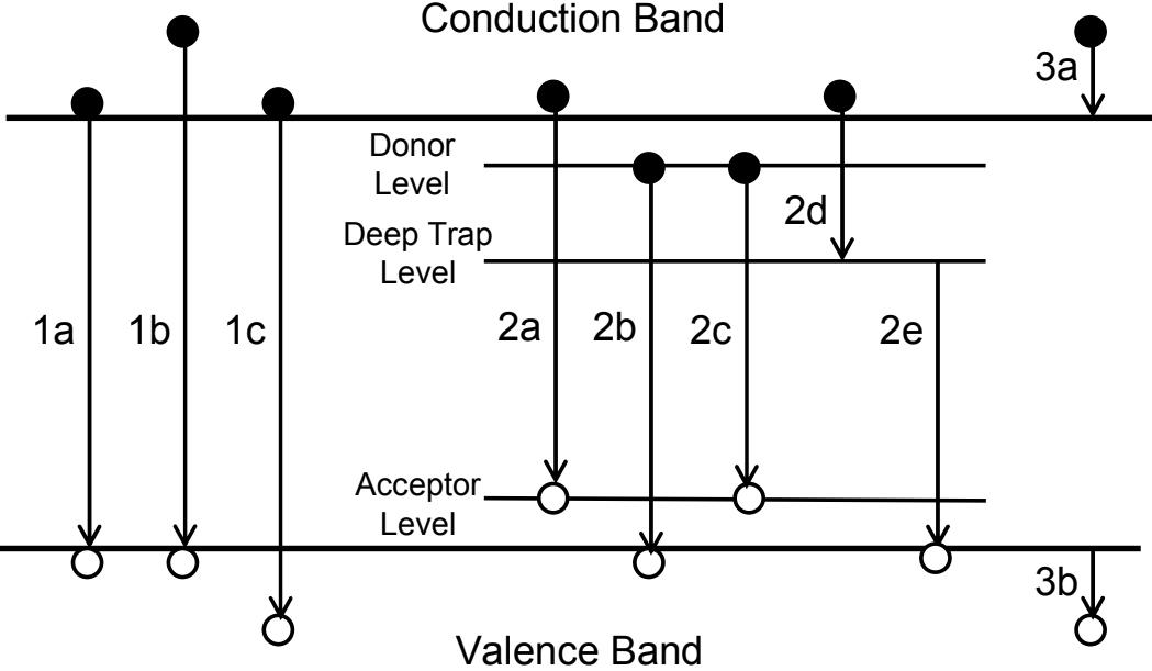
Figure 953. Radiative transition processes in silicon devices. Adapted from [1]. |
[1] Ivey HF, "Electroluminescence and Semiconductor
Lasers", IEEE J Quantum Electronics, Vol QE-2, No. 11,
pg 713-726, 1966.
|
