Chapter/Index: Introduction | A | B | C | D | E | F | G | H | I | J | K | L | M | N | O | P | Q | R | S | T | U | V | W | X | Y | Z | Appendix
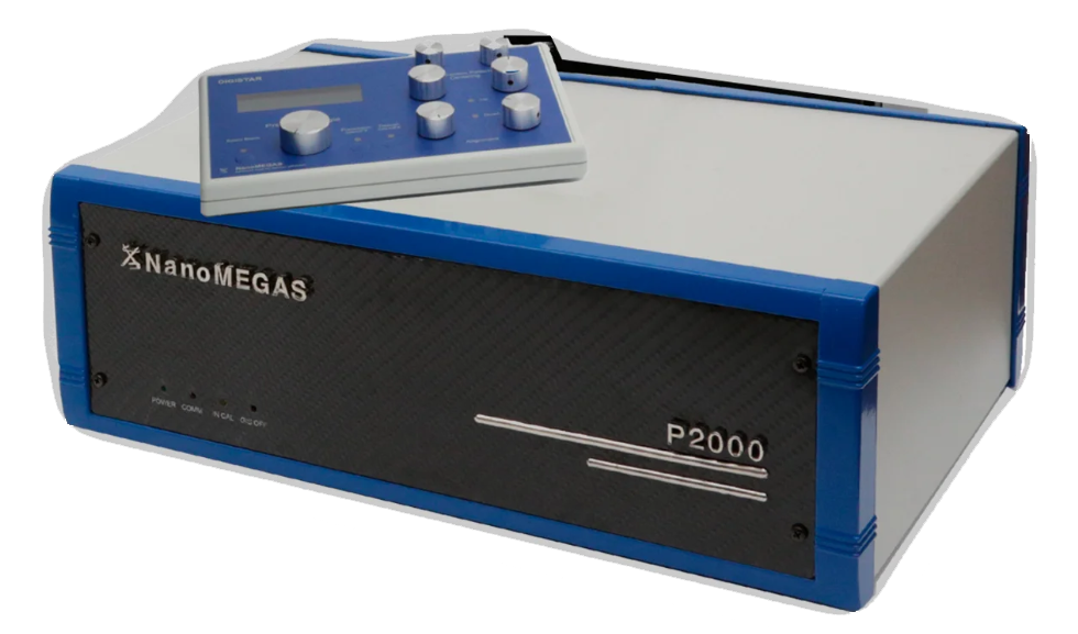
| Figure 1175a shows a NanoMEGAS controller, such as the DigiSTAR precession device, which is designed to integrate with Transmission Electron Microscopes (TEMs) to facilitate advanced electron diffraction techniques. These controllers typically feature a compact, rectangular chassis with a front panel that includes various control knobs, buttons, and indicators for precise operation. The design emphasizes functionality and ease of integration with existing TEM systems.
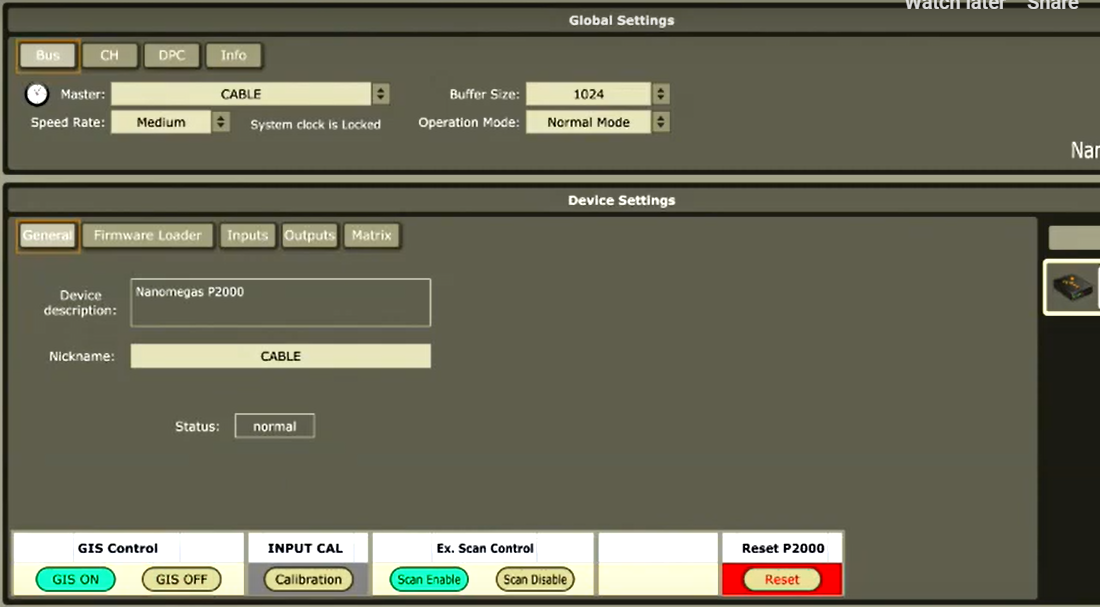
Figure 1175b shows the NanoMEGAS software interface, and Table 1175 lists the specifications of NanoMEGAS systems.
Table 1175. Specifications of NanoMEGAS systems.
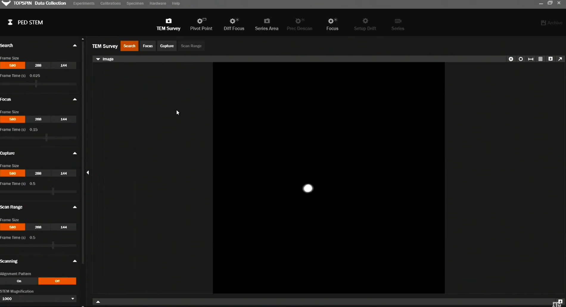
Figure 1175c shows the Topspin - NanoMEGAS interface. Topspin is a comprehensive digital framework designed to enhance Transmission Electron Microscopy (TEM) capabilities by integrating Scanning Transmission Electron Microscopy (STEM), beam precession, and advanced analytical experiments. Developed through a collaboration between AppFive and NanoMEGAS, Topspin enables scientists to obtain detailed nanoscale information with improved ease of use. The key features of Topspin include:
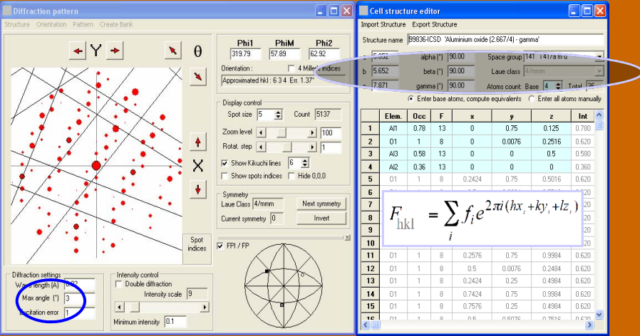
The ASTAR software package is a specialized tool designed to utilize the capabilities of 4D-Scanning Transmission Electron Microscopy (4D-STEM) by integrating beam precession technology. This software enables precise phase and orientation mapping at the nanoscale, essential for identifying and analyzing crystalline and amorphous structures within various materials. ASTAR's functionality includes phase mapping, which differentiates phases based on crystallographic patterns, and strain analysis, which reveals subtle distortions within the crystal lattice. By utilizing precession-assisted 4D-STEM, ASTAR reduces the effects of dynamical scattering, a common challenge in diffraction-based analysis. This approach improves the accuracy and reliability of the diffraction patterns, allowing users to obtain high-quality data critical for applications such as failure analysis and strain measurement in semiconductor devices. Additionally, the software is configured to integrate seamlessly with advanced electron microscopes, allowing for real-time data acquisition and on-the-fly data processing. This level of automation and user-friendliness minimizes operator intervention, streamlining complex analysis tasks and making high-precision nanostructural characterization more accessible across research and industrial settings. ASTAR®, [3] a patented tool and technique, operates in coordination with the DigiSTAR precession electron diffraction (PED) device to produce high spatial resolution orientation and phase maps, achieving resolutions between 1-4 nm for FEG TEM and under 10 nm for TEM-LaB6. It is compatible with most commercial TEMs (120-300 kV), including single and double Cs aberration-corrected TEMs, and can be connected to multiple TEMs within the same laboratory using an advanced galvanic isolation system (GIS) for secure ASTAR-TEM interfacing. ASTAR performs 4D-SPED (scanning precession electron diffraction) by synchronizing with beam precession to capture PED pattern series, eliminating the need for a STEM unit. It works with various diffracting materials (inorganic and organic) prepared by standard TEM specimen techniques. The system’s dedicated external CCD camera allows high-speed acquisition of electron diffraction (ED) patterns, typically achieving 100 ED patterns per second. For even higher acquisition speeds (>1000 fps), ASTAR can interface with high-end direct electron detectors. Post-acquisition, ASTAR generates virtual BF/DF images with user-defined apertures (disk, circle, line) and enables mask combinations (addition/subtraction) on ED patterns to highlight specific sample features. Additionally, it can produce diffraction pattern cross-correlation maps, offering insights into sample characteristics like grain thickness variation, domain boundary thickness, grain overlaps, and 3D structural details. ASTAR provides grain boundary generation in orientation and phase maps, including special boundaries with calculated grain size distribution, pole figure visualization for texture analysis, and 180° ambiguity correction for specific grain orientations. Used in conjunction with TOPSPIN, ASTAR supports the simultaneous acquisition of orientation, phase, strain, and STEM maps. NanoMEGAS's beam precession technology is typically implemented as a module in a separate computer attached to conventional (S)TEM electron microscopes, allowing it to function independently with its dedicated ASTAR software package for phase and orientation mapping and strain analysis. DiffGen 2, as shown in Figure 1175d, is a software tool designed to generate diffraction patterns for various crystal structures. It allows users to input specific parameters of a crystal structure, such as lattice constants, space group, and atomic positions, to simulate and visualize the corresponding diffraction patterns. This capability is particularly useful for researchers and students in crystallography and materials science, as it aids in understanding and interpreting experimental diffraction data. By providing the necessary crystal structure parameters, DiffGen 2 can create accurate representations of diffraction patterns, facilitating the analysis of material properties and behaviors. This tool is often used in conjunction with experimental techniques to validate findings or predict diffraction outcomes for hypothetical structures.
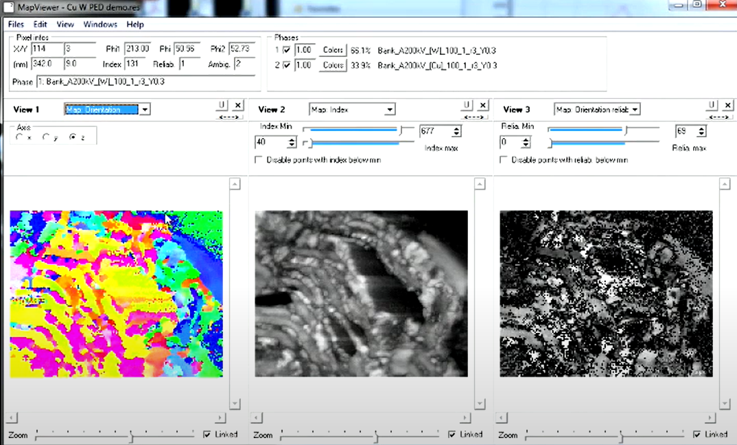
MapViewer as shown in Figure 1175e is a software tool designed for visualizing and analyzing crystallographic orientation data, commonly used in materials science and engineering. It processes data from techniques like Electron Backscatter Diffraction (EBSD) to generate orientation maps, pole figures, and inverse pole figures, aiding in the study of material properties and behaviors. The key features of MapViewer include:
[1] Advanced Tools For Electron Diffraction.
|