EDS Measurement of Zinc (Zn) - Practical Electron Microscopy and Database - - An Online Book - |
|||||||||||||
| Microanalysis | EM Book http://www.globalsino.com/EM/ | |||||||||||||
| ================================================================================= | |||||||||||||
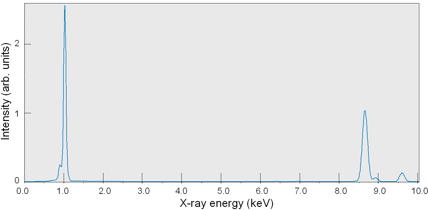
Figure 1317 shows an EDS spectrum of a pure zinc (Zn) material.
Figure 1317. EDS spectrum of a pure zinc material.
For thick TEM samples, k-factor correction due to X-ray absorption is needed in order to accurately quantify EDS measurements. Table 1317 lists examples of thicknesses at which the thin-film approximation is no longer valid due to X-ray absorption effects in specific materials. In the Al-7% Zn case, the Zn X-rays are not absorbed because of the higher energy of its X-rays.
|
|||||||||||||
| ================================================================================= | |||||||||||||
|
|
|||||||||||||