=================================================================================
OBIRCH (Optical Beam Induced Resistance CHange) is one type of Thermal Laser Stimulation (TLS) techniques and was developed in the early nineties by K. Nikawa and S. Inoue [1,2]. Later, IR-OBIRCH (Infra Red OBIRCH) has been a powerful fault isolation technology in integrated circuits (ICs). Especially, in many cases failure textures have been found with IR-OBIRCH technique but not with electrical measurements. IR-OBIRCH technique has been applied not only in test structures but also in final products.
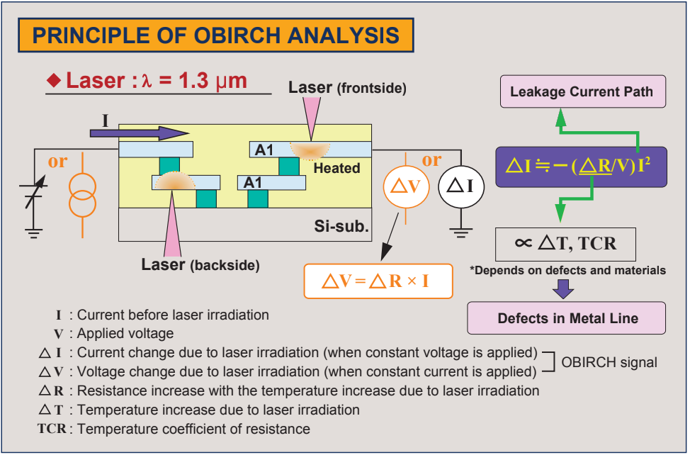
Figure 2852a. Principle of OBIRCH analysis. [18]
The OBIRCH technique has been widely applied to defect localization in ICs, for instance:
i) current alteration caused by leakage current paths,
ii) current alteration caused by
contact area resistance failure,
iii) detections of voids in Al lines [1, 5, 6] and Cu lines [7],
iv) voids under Al vias [6],
v) W vias [8],
vi) Cu vias [9],
vii) Si nodules [6],
viii) high-resistive area [10],
ix) current paths in metal test structures [1, 6] and in product ICs [11],
xi) metal bridging [14],
xii) high metal resistance [14],
xiii) metal line short [15],
xiv) gate oxide breakdown in pure gate oxide bulk without source and drain structures [15].
In leakage analysis with IR-OBIRCH, one node is connected to the Vbias port of the IR-OBIRCH Amplifier, while the other node is connected to the ground as shown in Figure 2852b. By a constant voltage on the Vbias port, the leakage current flows from Vbias to the ground in the Device Under Test (DUT). A scanning laser is used to irradiate and to heat (stimulate) the defect, junctions, metal traces, and via/contact connections, inducing a current variation (ΔIbias). ΔIbias can be given by,
ΔIbias = -(ΔRΔT/Vbias)I2 ---------------------------- [2852a]
where,
ΔRΔT -- The resistance change resulting from IR laser
beam scanning,
ΔT -- The temperature change resulting from IR laser
beam scanning.
ΔR is a function of ΔT and TCR (thermal coefficient of resistance). ΔIbias can be further given by,
ΔIbias = - TCR*ΔT*(Vbias/R0)
---------------------------- [2852b]
where,
R0 -- The resistance of the IC.
This heating generates a small electrical resistivity change that is usually constant everywhere if no failure is present. However, when a failure is present, the thermal spreading and the resistivity will be higher or lower depending on the thermoelectric behavior of the defective location. Finally, the extracted resistance change induced by the laser scanning is converted to form an image, highlighting the high current path. The electrical current is detected and amplified with an OBIRCH amplifier. The amplifier is operated in AC-coupled mode so that only the current variations are recorded to show defective locations. Analog signal is then coded with certain bits (e.g. 212) and transformed into digital values with acquisition card. OBIRCH signal amplitude can be displayed on screen in grey scale (e.g. from 0 to 4095) in a certain spatial resolution (e.g.1024 x 1024). Maximal positive and negative variations are displayed respectively in different colors (e.g. white and black, or red and green) as shown in Figure 2852c. Therefore, the OBIRCH image can be obtained as a two-dimensional (2D) map of the ΔI. Different from OBIC/EBIC technique, OBIRCH mainly detects failures in metallization wiring.
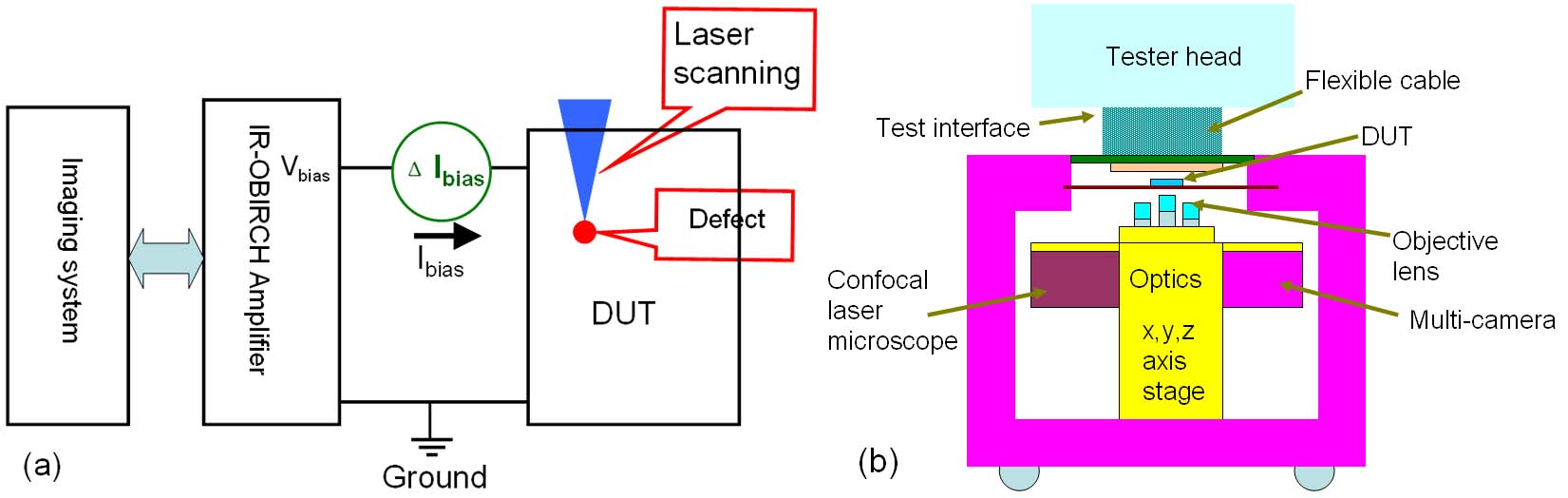
Figure 2852b. Schematic illustration of common IR-OBIRCH setup.
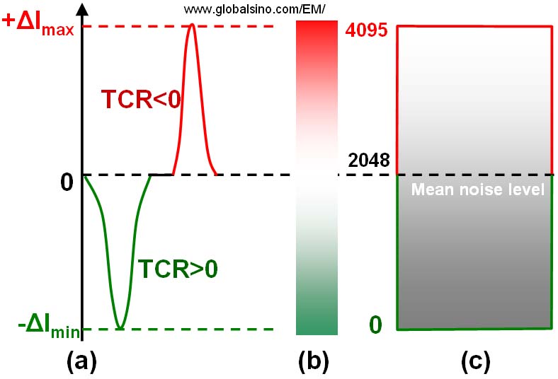
Figure 2852c. (a) Current variation (ΔIbias), (b) Superimposed colors, and (c) Coded IR-OBIRCH signal (ΔN).
In OBIRCH measurements, a laser with a wavelength of 1.34 µm is normally employed to avoid creating electron-hole pairs [3]. The light has a lower energy than the Si band gap (Eg = 1.12 eV) so that the probability of electron-hole pair generation is low and absorption occurs as conversion of light into heat. Note that electron-hole pairs induce photo-current that is strong noise against the OBIRCH signal. These optical properties allow performing frontside and backside analysis through Si thickness. However, in some cases lasers with shorter wavelengths (e.g. 633 nm [16]) are also used. Most OBIRCH systems limit the detection of circuits with maximum power supply voltage of 25V and current limit of 100 μA, or maximum voltage of 10 V and current limit of 100 mA. However, some OBIRCH systems have the capability of measuring circuits supplied with maximum voltage of 250 V and current of 6.3 A. [4] It was also proposed [4] that lock-in IR-OBIRCH can improve signal noise ratio (SNR) by employing a laser that is modulated by frequencies of 5 KHz or 50 KHz. The IR-OBIRCH can detect defects and current paths from the backside of Si chips because of weak attenuation (relatively transparent) of 1.34 µm wavelength laser in Si.
The sensitivity of defect detection using OBIRCH depends on the applied voltage and interconnect resistance. Serious defects, which change the resistance drastically, are detectable at higher voltages, while small defects, such as pits, can be found at low voltages (e.g. 0 V) [16, 17]. Furthermore, the sensitivity has also been improved at lower temperatures [12], by using a constant current source instead of a constant voltage source [10], by combining laser-modulation with lock-in amplifier [10], and by using a pre-amplifier [13].
However, OBIRCH is basically a DC-method, which sometimes limits the investigation of dynamically functional devices.
[1] Kiyoshi Nikawa and Shoji Tozaki, ISTFA
proceedings 1993 (ASM International), pp.303-310.
[2] Kiyoshi Nikawa and Shoij Inoue, "LSI failure
analysis using focused laser beam heating"
ESREF proceedings 1995 (Adera, France), pp.
307-312.
[3] Chunlei Wu, Masuda Motohiko, Winter Wang, Grace Song, Jinglong Li, Joe
Yu et al., “A Novel and low-cost Method to Detect Delay Variation by
Dynamic Thermal Laser Stimulation,” IRPS 2011, pp. 765–769.
[4] Chunlei Wu, Li Tian, Miao Wu, Diwei Fan, Lock-in IR-OBIRCH Assisted with Current Detection Probe Head Extend Its Application to High Voltage High Current Failure Analysis, 19th IEEE International Symposium on the Physical and Failure Analysis of Integrated Circuits (2012).
[5] Nikawa, K. et al. ISTFA, USA, p.11 (1994).
[6] Nikawa, K. et al., JJAP, 34, part 1, No. 5A p.2260 (1995)
[7] Tagami, M. et al. LSITS, Osaka, Japan, p.269 (2002).
[8] Yokogawa, S., et al., Microelec. Reliab. 41, p.1409 (2001).
[9] Yokogawa, S. et al., RCJ Reliab. Symp. Tokyo, p.51 (2002).
[10] Nikawa, K. and Inoue, S., ATS, IEEE, Japan, p.214 (1997).
[11] Nikawa, K. and Inoue, S., IRPS, IEEE, USA, p.346 (1996).
[12] Kawamura, N., et al., IEICE Trans. Elec. E77-C, p.579 (1994).
[13] Namura, T., et al., LSWS, Osaka, Japan, p.193 (2001).
[14] K. Nikawa, S. Inoue, K. Morimoto, S. Sone, “Failure analysis
case studies using the IR-OBIRCH (infrared optical beam
induced resistance change) method“, Test Symposium, 1999.
(ATS ‘99) Proceedings. Eighth Asian, 16-18 Nov. 1999, pp.
394-399.
[15] H.W. Yang, B.H. Lee, R.L. Hwang, L.H. Chu, D. Su, Novel IR-OBIRCH application in gate oxide failure analysis DOI:10.1109/IPFA.2004.1345633,
Physical and Failure Analysis of Integrated Circuits, 2004. IPFA (2004) Proceedings of the 11th International Symposium.
[16] M. Tagmi, T. Fukase, A. Matsumoto, M. Iguchi, Y. Hayashi and Y. Matsubara, A New Failure Observation in 0.10-µm-Wide Cu Lines Using Optical Beam Induced Resistance Changes (OBIRCH), Interconnect Technology Conference, Proceedings of the IEEE 2001 International (2001).
[17] K.Nikawa et al., 1996 Proc Int., 263, (1995).
[18] Overview of function of iPHEMOS series.
|