Practical Electron Microscopy and Database

An Online Book, Second Edition by Dr. Yougui Liao (2006)

Practical Electron Microscopy and Database - An Online Book

Chapter/Index: Introduction | A | B | C | D | E | F | G | H | I | J | K | L | M | N | O | P | Q | R | S | T | U | V | W | X | Y | Z | Appendix

TEM Imaging of Molybdenum Silicides

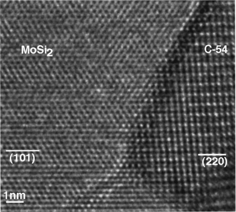
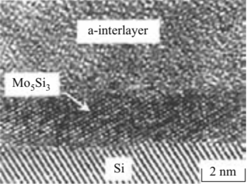
Table 991. TEM images of molybdenum silicides.

Molybdenum silicides TEM images
MoSi2 structure of MoSi2 C11 type
The structure of MoSi2 C11 type is based on close packed MeSi2-layer sequences of AB. The B positions are the saddle point positions of the metal atoms of the next layer.  
MoSi2 nucleated at the interface and acts as a template for epitaxial growth of C54 TiSi2
MoSi2 nucleated at the interface and acts as a template for epitaxial growth of C54 TiSi2. [1]  
Mo5Si3 Ti/Mo/Si sample after annealing at 500 °C for 30 s
Ti/Mo/Si sample after annealing at 500 °C for 30 s. [2]


[1] J. A. Kittl, M. A. Gribelyuk, and S. B. Samavedam, Mechanism of low temperature C54 TiSi2 formation bypassing C49 TiSi2: Effect of Si microstructure and Mo impurities on the Ti–Si reaction path, Applied Physics Letters, 73, 7, 900, 1998.
[2] Lih J. Chen, Silicide Technology for Integrated Circuits, 2004.