| Table 995. TEM images of nickel silicides.
| Nickel silicides |
TEM images |
| NiSi |
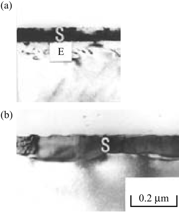
Residual defects formed in ion implanted silicon can be reduced by silicide formation. Figures above show the removal of end-of-range defects by NiSi formation on 110 keV, 5 × 10¹⁵/cm2 BF+2-implanted (001)Si: (a) as-deposited and (b) samples annealed at 600 °C for 1 h.
[5] |
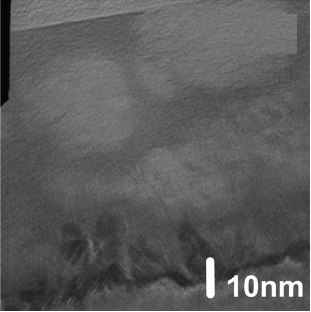
| NiSi + NiSi2 |
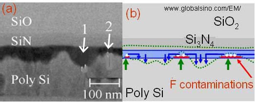
White arrow "1" points to thicker NiSi, while arrow "2" points to thinner NiSi2. Adapted from [4] |
| NiSi2 |
![Epitaxial silicide/Si interfaces, viewed in the [1-10] direction](image2/995i.PNG)
Epitaxial silicide/Si interfaces, viewed in the [1-10] direction: (a) the 7-fold type A NiSi2/Si(111) interface; (b) the 7-fold type B NiSi2/Si(111) interface and the 6-fold NiSi2/ Si(100) interface. Type A NiSi2 has the same orientation as the silicon substrate. Type B NiSi2 shares the surface normal <111> axis with the Si, but is rotated 180° about this axis with respect to the Si. [6]
|
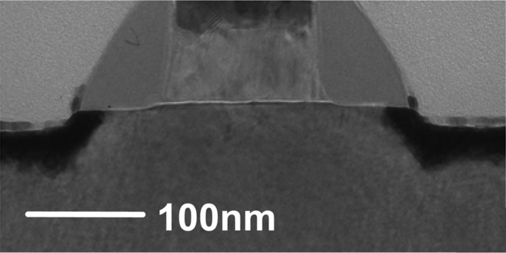
![(111) NiSi2 facet formed on the (100) Si plane. [1]](image2/995a.PNG)
(111) NiSi2 facet formed on the (100) Si plane, the facet induces junction leakage [1] |
Smooth silicide/Si interfaces with facetless texture of NiSi2 at the interface [1] |
 [1] [1]
 [2] [2]
 [2] [2]
 [2] [2]
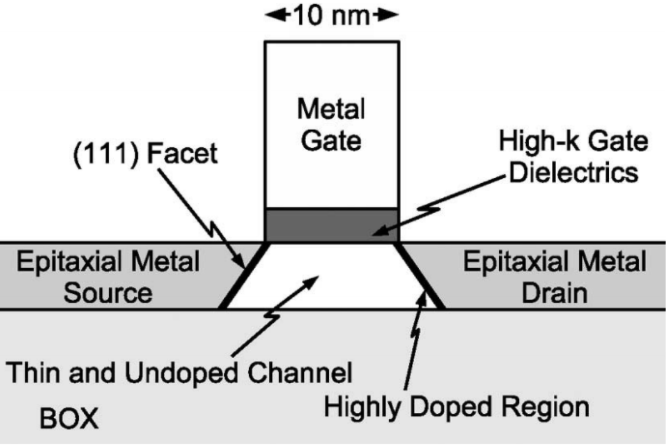
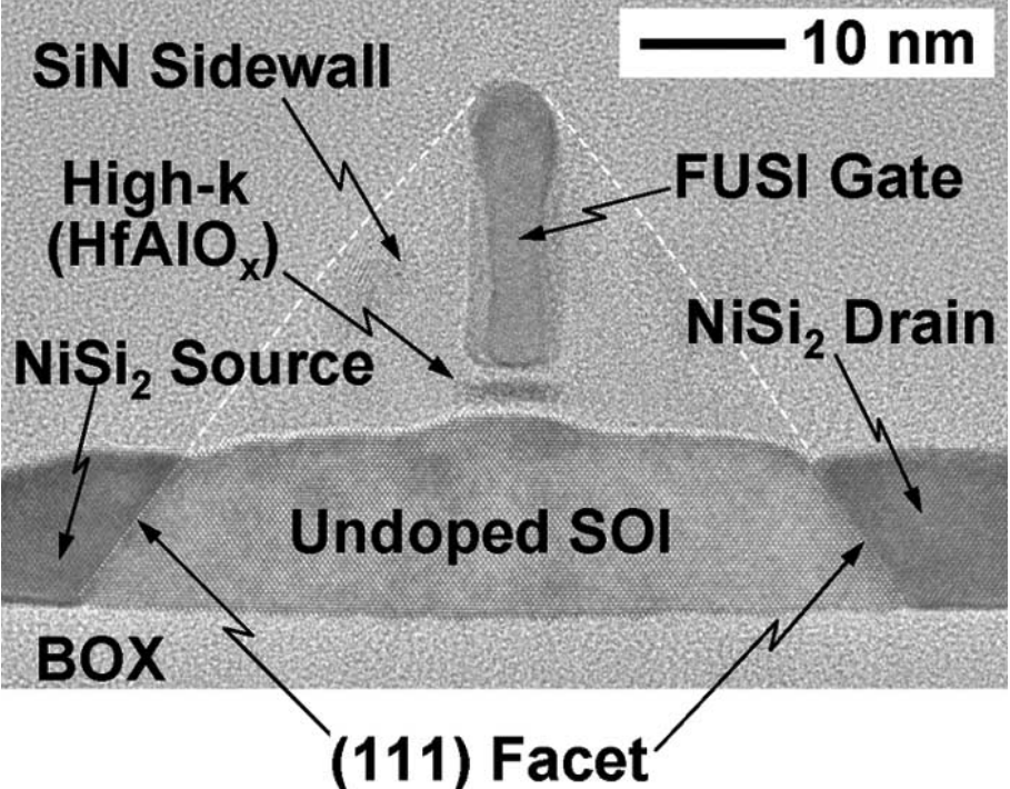
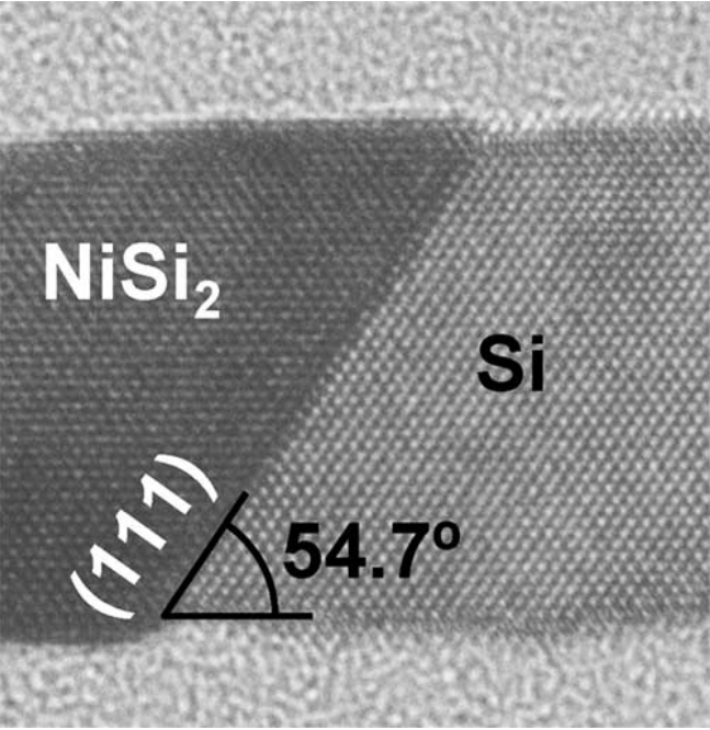
Self-organized (111) epitaxial NiSi2 S/D (with an angle of 54.7°) improves the short channel effect due to the trapezoidal shape channel formation. [2] |
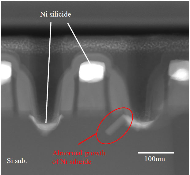
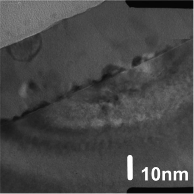
NiSi2 abnormal growth [3] |
| Ni0.23Si0.77 |
Rough silicide/Si interfaces [1] |
[1] Hou-Yu Chen, Chia-Yi Lin, Min-Cheng Chen, Chien-Chao Huang, and Chao-Hsin Chien, Nickel Silicide Formation using Pulsed Laser Annealing for nMOSFET Performance Improvement, Journal of The Electrochemical Society, 158 (8) H840-H845 (2011).
[2] N. Mise, S. Migita, Y. Watanabe, H. Satake, T. Nabatame, and A. Toriume, (111)-Faceted Metal Source and Drain for Aggressively Scaled Metal/High-k MISFETs, IEEE Trans. Electron Devices, 55, 1244 (2008).
[3] S. Kudo, Y. Hirose, N. Hashikawa, T. Yamaguchi, K. Kashihara, K. Maekawa, K. Asai, N. Murata, K. Asayama and E. Murakami, Analysis of Ni Silicide Abnormal Growth Mechanism Using Advanced TEM Techniques, IEEE International Reliability Physics Symposium, 2008. IRPS (2008) 10074334.
[4] Takuya Futase, and Hisanori Tanimoto, Fluoride Contamination Induced NiSi2 Film Formation in a Gate NiSi Line, IEEE Transactions on Semiconductor Manufacturing, 26(3), (2013) 355.
[5] Lih J. Chen, Silicide Technology for Integrated Circuits, 2004.
[6] R. T. Tung, Epitaxial CoSi2 and NiSi2 thin films, Materials Chemistry and Physics, 32 (1992) 107-133.
|
