| Figure 0112a shows an equivalent circuit of a power MOSFET with fixed capacitor symbols.

Figure 0112a. Another equivalent circuit of a power MOSFET. [1] |
Figure 0112b shows the equivalent circuit of a power MOSFET at turn-on process.
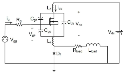
Figure 0112b. equivalent circuit of a power MOSFET at turn-on process. [1] |
Figure 0112c shows the MOSFET turn-on waveforms. This shows the initial delay as the gate voltage increases to the threshold, followed by a plateau as it charges the gate capacitance. The drain voltage starts high, then drops as the MOSFET turns on, allowing current to flow. The current remains zero during the delay, then ramps up as the MOSFET turns on, reaching a steady state at the end. MOSFET turn-on process consists
of different phases:
- Delay time period. This is the initial phase where the gate-source voltage (Vgs) is building up but has not yet reached the threshold voltage (Vth) needed to turn on the MOSFET.
At this stage, the gate drive voltage (Vgg) is applied, and the gate current (ig) flows through the gate resistor (Rg) to charge the gate-source capacitance (Cgs) and gate-drain capacitance (Cgd). The gate-source voltage Vgs increases exponentially, with a time constant determined by,
 ------------------------------------------------------ [0112a] ------------------------------------------------------ [0112a]
During this period, the drain current (Ids) is essentially zero, as the MOSFET channel has not yet formed. The load current continues to flow through the freewheeling diode (Df) in parallel with the MOSFET. The gate-source voltage during this time can be given by,
 ------------------------------------------------------ [0112b] ------------------------------------------------------ [0112b]
where t is the time elapsed, and Vgs(t) gradually approaches Vth. The delay time (td) is the time required for Vgs to reach Vth which can be calculated by,
 ------------------------------------------------------ [0112c] ------------------------------------------------------ [0112c]
- Rise time period. It is the phase where the gate-source voltage (Vgs) has reached the threshold voltage, allowing the MOSFET to begin conducting current. As soon as Vgs reaches the threshold voltage Vth, the MOSFET channel forms, allowing current to start flowing from drain to source. The drain current Ids begins to rise as Vgs continues to increase above Vth. This current rise is typically linear, defined by the MOSFET's transconductance gm. The drain current Ids can be given by,
 ------------------------------------------------------ [0112d] ------------------------------------------------------ [0112d]
where gm is the MOSFET’s forward transconductance.
During the rise time, Vds begins to drop as Ids increases. The increase in Ids causes the voltage across the load to increase, while Vds decreases due to the current’s flow through the MOSFET. Vds can be given by,
 ------------------------------------------------------ [0112e] ------------------------------------------------------ [0112e]
Ld and Ls represent the parasitic inductances of the drain and source, respectively, which impact the rate of change of Ids and thus Vds.
As
Vds
falls,
Cgd, the gate-drain capacitance, starts to discharge. This discharge path is critical, as it determines the rate at which
Vds
can decrease. The charging of Cgd can be modeled by,
 ------------------------------------------------------ [0112f] ------------------------------------------------------ [0112f]
Cgd influences the switching speed because it directly affects how fast Vds can change. The value of Rg, the gate resistance, is crucial during this period, as it impacts the time constant in Equation 0112a, determining how quickly Vgs rises.
The parasitic inductances Ld and Ls affect the dIds/dt rate. The higher the inductance, the slower the current change rate due to the energy storage in these inductive elements. The voltage drop across the inductances is given by,
 ------------------------------------------------------ [0112g] ------------------------------------------------------ [0112g]
VL contributes to the voltage drop along the current path, influencing the overall transient behavior during the rise time.
During the rise time, both
Vds
and Ids
are non-zero, resulting in switching losses as power is dissipated in the MOSFET. The instantaneous power loss can be approximated by,
 ------------------------------------------------------ [0112h] ------------------------------------------------------ [0112h]
The total energy loss over the rise time tr can be calculated by integrating the instantaneous power over this period,
 ------------------------------------------------------ [0112i] ------------------------------------------------------ [0112i]
The rise time
tr
depends on the gate resistance Rg, the input gate voltage
Vgg, and the transconductance
gm. tr can be give by,
 ------------------------------------------------------ [0112j] ------------------------------------------------------ [0112j]
The value of
tr
can be influenced by the input voltage
Vgg, the MOSFET characteristics such as
gm, and external factors like
Rg.
- Plateau time period. During this time, significant changes occur in both the drain current Ids and the drain-source voltage Vds. During the plateau phase, the gate voltage Vgs reaches a level where it is high enough to maintain the MOSFET in a conducting state but does not yet continue to increase linearly. This plateau in Vgs is due to the charging of the gate-drain capacitance Cgd, also known as the Miller effect. At this stage, the gate current Ig largely goes into charging Cgd rather than increasing Vgs. As Cgd charges, it impacts the rate of Vds decrease, causing Vds to fall more slowly compared to other periods. The drain-source voltage Vds decreases significantly during the plateau period, as the MOSFET transitions from the off state towards full conduction. This decrease in Vds coincides with the rapid increase in drain current Ids, allowing the MOSFET to support the load current fully. The Vds continues to drop as the gate-drain capacitance Cgd pulls charge until the MOSFET reaches the on-state voltage level. While Vgs is held constant, the drain current Ids continues to increase towards its final value. This is because the channel is forming and becoming conductive, allowing more current to flow through the MOSFET. The current increase is typically limited by the parasitic inductance Ld in the drain path and the load characteristics. The plateau period is a phase where significant power dissipation occurs due to the simultaneous presence of Vds and Ids. This results in switching losses in the form of heat within the MOSFET. These losses are known as "Miller losses" or "switching losses" and are proportional to the current, voltage, and the switching time during this period. The longer the plateau period, the more switching losses the MOSFET experiences. For this reason, the gate resistor Rg is often optimized to minimize the time spent in this phase. The duration of the plateau period depends on the gate drive strength, the gate-drain capacitance Cgd, and the gate resistor Rg. A higher Cgd or Rg increases the plateau duration, while a stronger gate drive (higher Vgg) can reduce it. The plateau time can be estimated based on the circuit parameters, as it is related to the charging time of Cgd and the Miller effect. During the plateau period, the gate current Ig is used to charge Cgd,
 ------------------------------------------------------ [0112k] ------------------------------------------------------ [0112k]
With the drain current increasing and Vds decreasing, the gate voltage remains nearly constant. The Vds reduction is governed by,
 ------------------------------------------------------ [0112l] ------------------------------------------------------ [0112l]
This phase concludes when Vds reaches its minimum on-state value, allowing Vgs to resume its increase.

Figure 0112c. MOSFET turn-on waveforms. |
[1] Hamed Raee, Ali Rabiei, T. Thiringer, 2013 8th IEEE Conference on Industrial Electronics and Applications (ICIEA), Analytical prediction of switching losses in MOSFETs for variable drain-source voltage and current applications, DOI: 10.1109/ICIEA.2013.6566458, 2013.
|
