Chapter/Index: Introduction | A | B | C | D | E | F | G | H | I | J | K | L | M | N | O | P | Q | R | S | T | U | V | W | X | Y | Z | Appendix
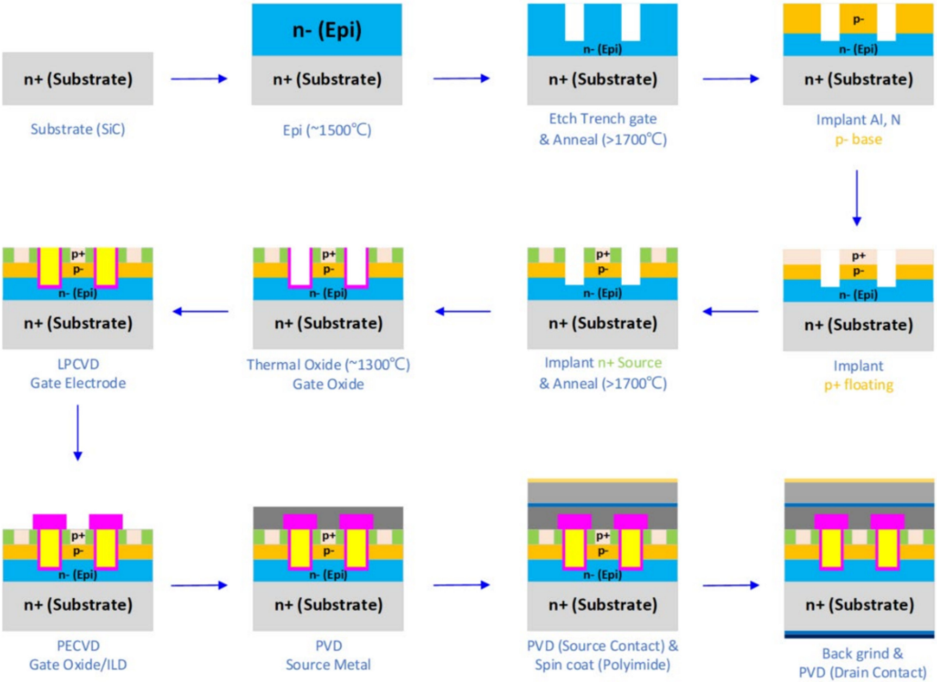
| Figure 0115 illustrates the process flow for fabricating a SiC trench MOSFET. The process begins with the epitaxial growth of the n- drift layer on an n+ substrate. The trench structure is then created, followed by p-base implantation. This is typically achieved using aluminum or nitrogen to define the p-base region within the trench. Next, a p+ shielding region is implanted to improve the device's robustness, followed by n+ implantations for the source and drain regions. High-temperature thermal oxidation is performed to grow a gate oxide layer, and subsequent annealing enhances its quality. Finally, the gate electrode, source metal, and drain metal are deposited, and the device is encapsulated with a polyimide passivation layer, which provides protection and enhances device performance by reducing defect density.
Figure 0115. SiC MOSFET process flow. [1]
[1] Catherine Langpoklakpam, An-Chen Liu, Kuo-Hsiung Chu, Lung-Hsing Hsu, Wen-Chung Lee, Shih-Chen Chen, Chia-Wei Sun, Min-Hsiung Shih, Kung-Yen Lee and Hao-Chung Kuo, Crystals, 12, 245, 2022.
|