Chapter/Index: Introduction | A | B | C | D | E | F | G | H | I | J | K | L | M | N | O | P | Q | R | S | T | U | V | W | X | Y | Z | Appendix
| Figure 0127a shows an EBAC test targeting a gate defect of CMOS image sensors. For two samples, S1 and S2, which are suspected to have damaged gates, the gate and source contacts are exposed and then a bias is applied. In images (a) and (c), acquired through conventional EBAC analysis, the entire component region is visible, making it difficult to pinpoint specific defect sites. Conversely, the DI-EBAC images (b) and (d) highlight localized response areas, with sizes ranging from 0.10 to 0.15 μm. The STEM image in Figure 0127a (f) shows the cross-sectional analysis results of the S1 sample region near the DI-EBAC reaction site. A short defect is observed between the W contact and the Si substrate. Electron-beam irradiation of short-circuit paths between various materials generates a thermoelectromotive force via the Seebeck effect, which is detected through current variations. This example confirms that DI-EBAC provides high resolution and serves as an effective tool for analyzing short defects.
Figure 0127b shows a DI-EABC image taken from an area with a metal short defect in a CMOS image sensor.
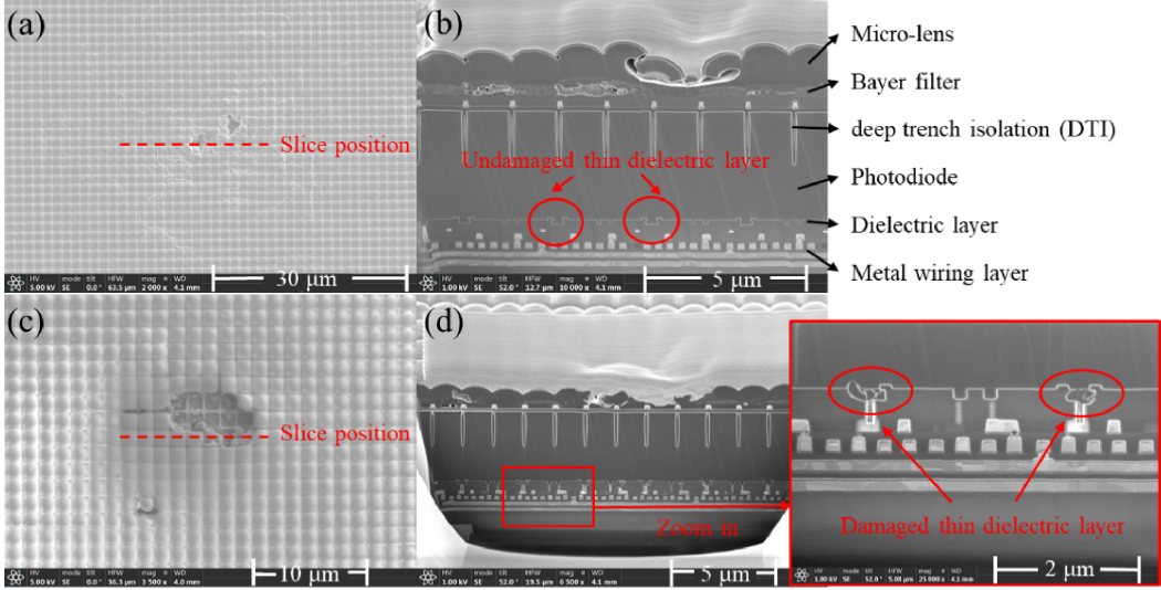
In Figure 0127c, the damaged cross-section of the CMOS Image Sensor (CIS) is examined using FIB and SEM. This analysis reveals the layered structure of the CIS and highlights the extent of damage induced by a 1550 nm nanosecond laser. The FIB cross-section images display the ablation of the micro-lens layer, along with the underlying Bayer filter, and indicate thermal degradation in the photodiode region. In areas with increased laser intensity, the damage extends deeper, compromising the dielectric layer between the photodiode and metal wiring. The SEM images provide further insight into the material disruption and failure points within these layers, showcasing the mechanical and thermal effects of laser-induced breakdown. Overall, this detailed cross-sectional view contributes to understanding the laser damage mechanisms at play, particularly regarding how different laser intensities affect various CIS components
[1] https://www.hitachi-hightech.com/global/en/sinews/si_report/130214/.
|