Chapter/Index: Introduction | A | B | C | D | E | F | G | H | I | J | K | L | M | N | O | P | Q | R | S | T | U | V | W | X | Y | Z | Appendix
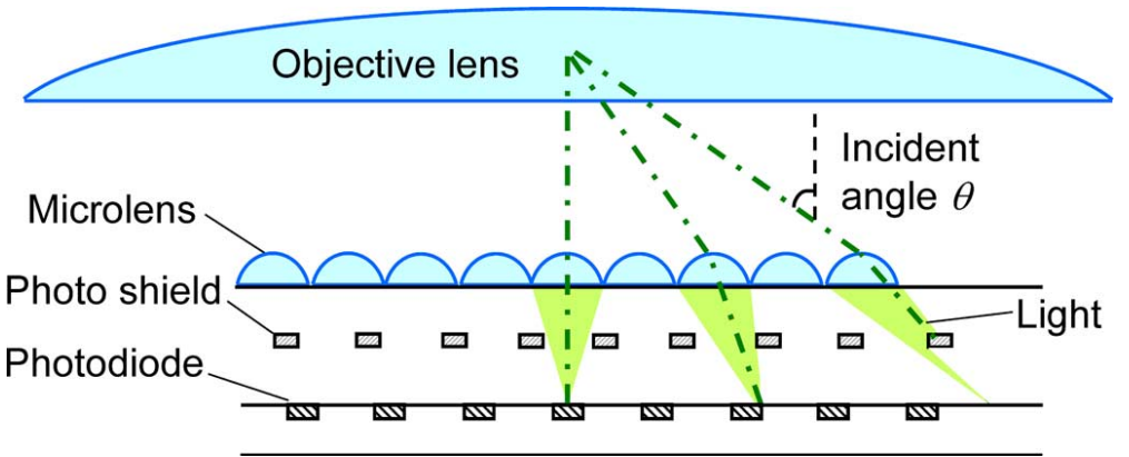
| The schematic in Figure 0130a illustrates a camera module equipped with an ultrashort focal objective lens. Due to the very short working distance of the lens, incident light enters at a steep angle, especially toward the periphery of the image sensor. This results in a decreased efficiency of light collection at the sensor's edges, as the high-angle light fails to focus effectively on the peripheral regions of the image sensor. This design challenge can limit overall image brightness uniformity across the sensor area.
In a MOS image sensor, a photo shield serves to block unwanted light from reaching specific areas of the sensor, particularly those that should not be light-sensitive, such as transistors, circuits, and interconnects. This prevents stray light from affecting the sensor's performance and ensures that only the photodiode (or pixel area) receives light. The photo shield is typically a layer of opaque material, such as metal, applied over these areas to protect against optical interference. By controlling light exposure in this way, the photo shield helps to reduce noise, enhance image quality, and improve overall sensor efficiency and reliability.
[1] Kazutoshi Onozawa, Kimiaki Toshikiyo, Takanori Yogo, Motonori Ishii, Kazuhiko Yamanaka, Toshinobu Matsuno, and Daisuke Ueda, A MOS Image Sensor With a Digital-Microlens, IEEE TRANSACTIONS ON ELECTRON DEVICES, VOL. 55, NO. 4, APRIL 2008.
|