Chapter/Index: Introduction | A | B | C | D | E | F | G | H | I | J | K | L | M | N | O | P | Q | R | S | T | U | V | W | X | Y | Z | Appendix
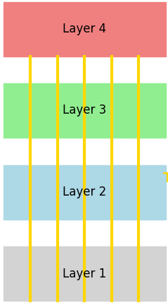
| 3D Integrated Circuits (3D ICs) mark a transformative approach in semiconductor design, addressing the limitations of traditional two-dimensional IC scaling. By stacking multiple layers of circuits and interconnecting them using Through Silicon Vias (TSVs), 3D ICs reduce the physical distances between logic, memory, and other components, significantly enhancing data transfer speeds and reducing power consumption. This architecture alleviates bandwidth bottlenecks by enabling shorter interconnects and greater parallelism, which is critical in applications requiring high-performance data processing, such as AI and mobile computing. Various 3D IC architectures, including stacked memory (e.g., HBM and HMC), memory-on-logic, and logic-on-logic structures, each offer unique advantages depending on the integration needs and design constraints. However, implementing 3D ICs is complex, with challenges in thermal management, yield, reliability, and power delivery. Heat removal becomes difficult as stacked layers increase heat density, especially for dies positioned farther from the heat sink. Innovations like microfluidic cooling channels are being explored to counter this. Additionally, the TSV fabrication process can introduce stress into the silicon, impacting reliability and performance. Testing 3D ICs also presents difficulties, as defects in any layer can compromise the entire stack, reducing overall yield. Industry solutions focus on refining TSV processes and adopting wafer-level testing to manage yield and reliability. Despite these challenges, 3D ICs hold promise for next-generation computing, driving continued research and investment in this transformative technology. Figure 0145a illustrates the architecture of a 3D Integrated Circuit (3D IC), showcasing multiple layers stacked vertically, each representing a distinct function such as logic, memory, or sensor components. These layers are interconnected by Through Silicon Vias (TSVs), which are shown as vertical channels traversing the layers. TSVs play a critical role in 3D ICs by facilitating high-bandwidth communication between layers while significantly reducing the length of interconnects. This design enables more efficient data transfer, decreases latency, and reduces power consumption compared to traditional 2D ICs. The image captures the foundational concept of 3D ICs, emphasizing the compactness and improved performance achievable through vertical integration. The integration of various functionalities within a single, stacked package further demonstrates the advantages of 3D ICs in advancing computational efficiency and form factor, especially for high-performance applications like artificial intelligence and mobile computing.
|