Chapter/Index: Introduction | A | B | C | D | E | F | G | H | I | J | K | L | M | N | O | P | Q | R | S | T | U | V | W | X | Y | Z | Appendix
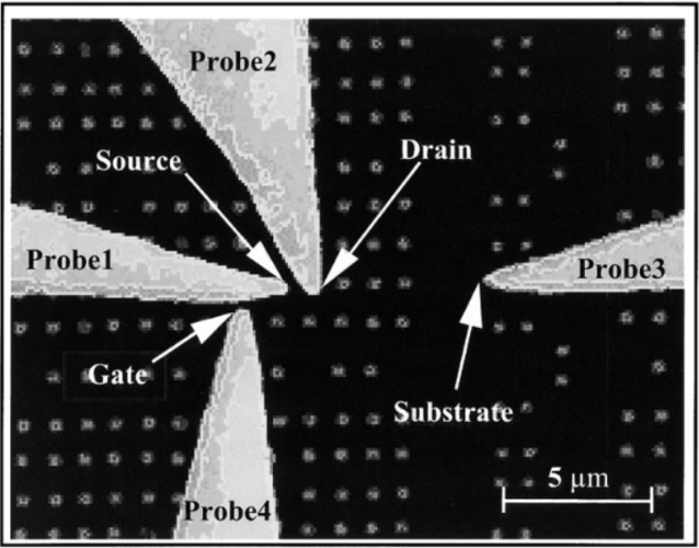
| Figures 0161a, 0161b, and 0161c present the application of the nanoprober technique for directly measuring the MOS characteristics of failed SRAM memory cells. Figure 0161a displays an SEM image of the nanoprober setup within a microprocessor, illustrating how finely positioned probes in the SEM environment allow direct, in-situ measurements on specific transistors, particularly failure bits. This capability is critical for accessing precise failure points. In Figure 0161b, the Ids-Vgs curve shows a marked reduction in the drain current (Ids) for the PMOS transistor in the failure bit, which measures nearly an order of magnitude lower than that of a typical functioning bit, indicating a significant drop in current drive capability associated with the failure mode. The drain current of the PMOS was approximately an order of magnitude lower. Similarly, Figure 0161c presents the transconductance (Gm) versus gate voltage (Vg) characteristics, where the failed bit’s transconductance is diminished compared to that of a normal bit. This shows that the threshold voltage was around 1 V higher than that of normal bits. This reduction aligns with a higher threshold voltage and reduced current, reinforcing the hypothesis of local gate depletion contributing to the SRAM failure. Therefore, the nanoprobing data emphasize how nanoprober measurements reveal critical electrical disparities between functional and failed memory cells, enabling a deeper understanding of the failure mechanism at a device level.
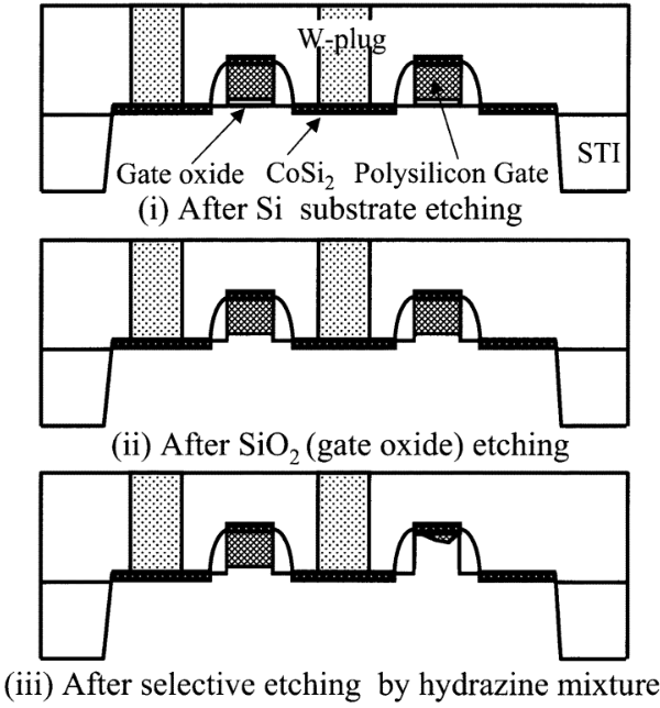
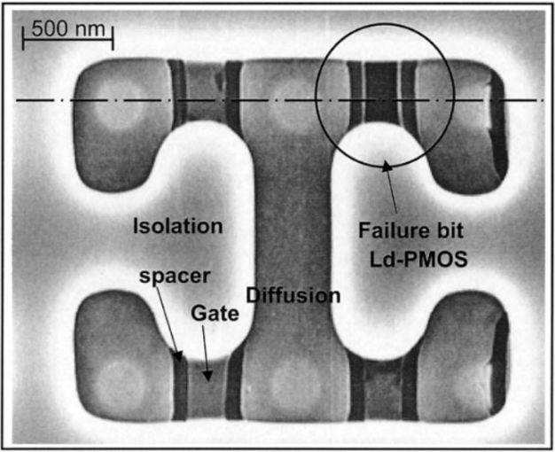
Figures 0161d and 0161e illustrate the selective etching technique using a hydrazine mixture, highlighting the local gate depletion and the presence of a large grain in the PMOS gate poly-Si of the failure bit. Figure 0161d shows the sample preparation flow for hydrazine selective etching, and Figure 0161e provides an SEM photograph demonstrating the result, where the gate polysilicon of the failure bit is etched off completely, unlike the normal bit. These figures support the finding that minimizing grain size in the gate poly-Si improves drain current degradation and suppresses this failure mode.
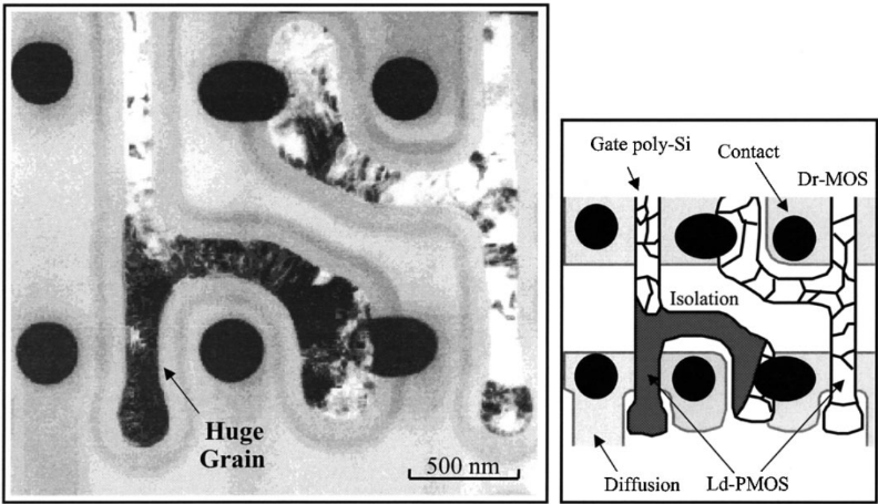
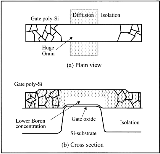
Figure 0161f presents a TEM (Transmission Electron Microscope) photograph of the failed bit, alongside an image illustrating the grain structure in the gate polysilicon of the failure bit. It reveals a large grain, exceeding 1 µm in size, lying on the active channel region of the PMOS transistor. This oversized grain is highlighted as a significant factor contributing to boron depletion within the polysilicon gate, which, in turn, results in reduced PMOS drain current (Ids) and contributes to SRAM cell failures. Dr-MOS typically refers to the driver MOSFET in the SRAM cell, which is responsible for driving the output or stabilizing the bit stored in the cell. In SRAM circuits, Dr-MOS devices are crucial for maintaining data stability during read and write operations. Ld-PMOS stands for the load PMOS transistor in the SRAM cell. The Ld-PMOS provides a load to the cell and plays a role in maintaining the voltage at the storage nodes, essential for the retention of data in the SRAM cell. The characteristics of the Ld-PMOS, such as its threshold voltage and transconductance, significantly influence cell stability, especially under low-voltage and high-frequency operation conditions.
Figure 0161g presents a schematic representation of boron depletion in large grains of gate polysilicon. It illustrates how boron atoms first diffuse through the grain boundaries and then into the grains themselves. In smaller grains, boron diffusion is relatively uniform across the gate electrode. However, in larger grains, boron diffusion is suppressed, leading to depletion in certain areas, which in turn results in local gate depletion. This depletion reduces the drain current (Ids) of the PMOS transistor, contributing to the failure mechanism observed in the SRAM cells.
[1] Ikeda, S., Yoshida, Y., Ishibashi, K., & Mitsui, Y., Failure Analysis of 6T SRAM on Low-Voltage and High-Frequency Operation. IEEE Transactions on Electron Devices, 50(5), 1270–1276, 2003.
|