| The failure analysis procedure for identifying the complex SRAM defects presented in Figure 0171a involved several systematic steps below:
-
Initial Diagnosis and Correlation Analysis: The analysis began with an electrical diagnosis that indicated increased supply current in failing devices, correlated with a specific fail pattern along bit lines (BL) at the SRAM block edges. The failure depended on SRAM supply voltage. This pattern initially suggested a potential SRAM peripheral issue as shown in Figure 0171a. That is, this map displayed failing bits concentrated along the edges of each SRAM block, a pattern often characteristic of peripheral circuit problems, such as issues in the sense amplifier or other I/O circuitry.

Figure 0171a. Example of a fail bit map showing failing bits as black-filled squares located along the edges of each SRAM block. [1] |
-
Global Localization Techniques:
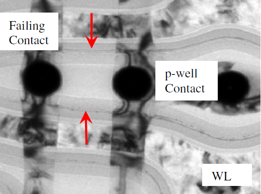
- Thermal Laser Stimulation (TLS): TLS was used to locate emission spots in the failing regions. An overlay of the TLS and optical images showed emission spots correlated with failing bit line contacts, particularly near H-shaped p-well regions. This step revealed an unexpected defect in the cell area rather than the periphery as shown in Figure 0171b.

Figure 0171b. TLS imaging with a backside optical image, showing emission spots near SRAM cell regions and the periphery. The TLS image (bottom left) highlights specific failure areas correlating with bit line (BL) contacts near H-shaped p-well regions, with spot intensity varying due to leakage current differences across failing contacts. [1] |
-
Passive Voltage Contrast (PVC) and Atomic Force Prober (AFP):
- SEM Passive Voltage Contrast (PVC): This imaging technique highlighted a bright line on M1 (the first metal layer), indicating a leaky BL contact.
- AFP Current Imaging: AFP was employed to obtain current leakage images, confirming the presence of leakage at the failing BL contact.
- Physical Analysis with Focused Ion Beam (FIB) and Transmission Electron Microscopy (TEM):
- Layer-by-Layer Inspection: The failed chip was polished layer-by-layer down to the bit line level (M2) for detailed optical and scanning electron microscopy (SEM) inspections. SEM at the M1 layer revealed bright contrasts, signifying leaky BL contacts.
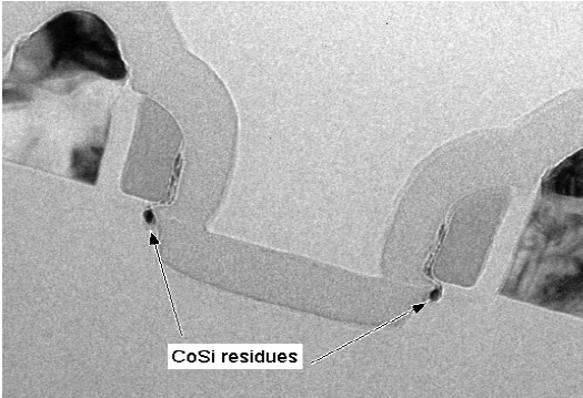
- High-Angle Annular Dark Field (HAADF) STEM: HAADF STEM imaging detected strong material contrast, particularly for CoSi, and ultimately uncovered CoSi residues on spacer walls of WLs. These residues were bridging the failing contact to the adjacent p-well contacts, creating a horizontal leakage path.
- Hypothesis Confirmation as shown in Figure 0171c:
- TEM Lamella Analysis: Thin and thick TEM lamellae were prepared to investigate the leakage path in greater detail. The surface-parallel TEM confirmed the presence of CoSi "stringers" bridging the contacts along the WLs. That is, the failure mechanism involves a unique bridging defect within the SRAM cells due to cobalt silicide (CoSi) residues. These residues formed "stringers" along the word lines (WLs) of the SRAM cells, which bridged neighboring active areas. The CoSi residues were observed on the spacer walls and beneath the spacers in the SRAM cells, connecting the failing bit line (BL) contact with adjacent p-well contacts.
- Process Adjustment: Based on these findings, the fab adjusted the CoSi process parameters to mitigate residue formation, leading to a significant yield improvement.
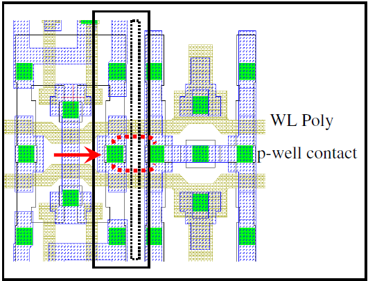
Figure 0171c. (a) The dotted red lines indicate the horizontal leakage path along the WL poly. The red arrow highlights the failing contact. The black-lined box marks the position of the thick lamella, and the dotted line outlines the location of the thin lamella. (b) The TEM image of a thick lamella reveals CoSi residues along the spacer wall, as indicated by the red arrows. (c) An image of a thin TEM lamella above the STI distinctly reveals CoSi residues, highlighted by red arrows. And (d) Surface-parallel TEM imaging validated the hypothesis, revealing a CoSi stringer aligned with the word line between two contacts. [1] |
Overrall, this horizontal bridging created unintended conductive paths that led to leakage. Interestingly, this defect was initially thought to be a peripheral SRAM issue (such as a sense amplifier problem), but further analysis revealed it was located in the cell region. This bridging defect resulted from process variations in the CoSi layer, leading to increased leakage currents and significant yield loss. Adjusting the CoSi deposition process in the fab mitigated this issue, ultimately improving yield.
[1] Zhongling Qian, Frank Siegelin, Birgit Tippelt, Stefan Müller, Localization and physical analysis of a complex SRAM failure in 90nm Technology, Microelectronics Reliability, 46, 1558–1562, 2006.
|