| Figure 0174a illustrates the layout and equivalent circuit of a 6T SRAM cell embedded in a 0.25-μm generation microprocessor. [1] The left side of the figure shows the physical layout of the SRAM cell, and the right side shows the equivalent circuit schematic. This SRAM cell design is used in an application for high-frequency and low-voltage modes.

Figure 0174a. 6T SRAM cell layout embedded on a 0.25-μm generation microprocessor (left) and its equivalent circuit (right). Adapted from [1] |
The 6T SRAM cell stores a single bit of data by holding it in a stable state within a cross-coupled inverter pair. Table 0174 shows the truth table for such a 6T SRAM cell.
Table 0174. Truth table for such a 6T SRAM cell presented in Figure 0174a.
| Operation |
Tr-NMOS Gates |
Drain of Tr-NMOS |
Drain of Tr-NMOS |
Node Q |
Node QB |
| Tr-NMOS |
WL (Word Line) |
Tr-NMOS |
BL (Bit Line) |
Tr-NMOS |
BLB (Bit Line Bar) |
| Hold |
Off |
Low |
|
— |
|
— |
Stable (either 0 or 1) |
Stable (either 0 or 1) |
| Read '1' |
|
High |
|
High |
|
Low |
High |
Low |
| Read '0' |
|
High |
|
Low |
|
High |
Low |
High |
| Write '1' |
|
High |
|
High |
|
Low |
High |
Low |
| Write '0' |
|
High |
|
Low |
|
High |
Low |
High |
In details, the operation steps during a write operation to "1" are:
- Assume Q = 0, QB = 1, BL = High, BLB = Low, WL = Low.
- BL and BLB are input.
-
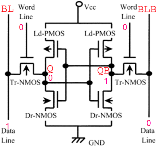
Figure 0174b. Initial state of the 6T SRAM before writing "1". |
-
Now set WL = High.
-
BLB = Low (ground) so that QB voltage decreases as shown in Figure 0174d.
-
If the QB voltage goes lower than the threshold voltage of M2 in Figure 0174a, then M2 will be off and M1 will be on as shown in Figure 0174c. Then, the output Q is 1.
- Therefore, Q is written to "1" from initial state of "0".
- The key of writing Q to "1" was that the BLB was forced to be "0".
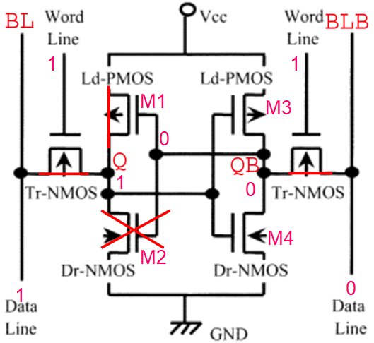
Figure 0174c. A transition state of writing "1". |
-
and then QB
will be 0, and then Q will be 1.
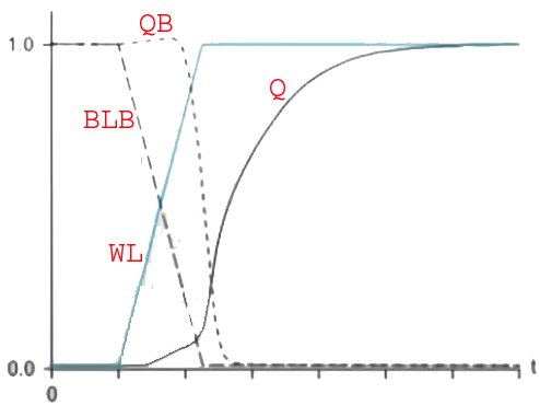
Figure 0174d. Waveform during the operation step of writing to "1". |
-
On the other hand, there is a design issue.
If the capacitor on the left starts to "1" due to discharge, then the voltage at Q increases
and
will be greater than the threshold voltage
of M4 so that M4 will be on. Then, QB will be "0".
Therefore, in design, we need to make sure that
the voltage at Q does not exceed
the threshold voltage
of M4. That means, we need to make sure Q and QB are not at "0" at the same time.
During a write "0" operation in the 6T SRAM cell shown in Figure 0174a, the transistors behave as follows:
- Activated Transistors:
- The access transistors (Tr-NMOS) on both sides are activated by asserting the Word Line (WL), allowing the bit lines (Data Lines) to connect to the internal storage nodes.
- The driver NMOS transistor (Dr-NMOS) on the side where "0" is being written is activated, pulling that storage node to ground, ensuring the "0" state.
- The load PMOS transistor (Ld-PMOS) on the opposite side (where "1" is stored) is on to keep that side at Vcc, thereby reinforcing the cross-coupled inverter configuration.
- Non-Activated Transistors:
- The driver NMOS transistor (Dr-NMOS) on the side where "1" is stored remains off, as it does not need to pull the node to ground.
- The load PMOS transistor (Ld-PMOS) on the side where "0" is being written is off, since this node is already grounded by the active Dr-NMOS transistor on that side.
The transistors that are activated and not activated during a write "0" operation are different from those during a write "1" operation in the 6T SRAM cell:
- During Write "0":
- Activated:
- Access transistors (Tr-NMOS) on both sides (because the Word Line is activated).
- Driver NMOS (Dr-NMOS) on the side where "0" is being written (to pull that storage node to ground).
- Load PMOS (Ld-PMOS) on the opposite side where "1" is retained (to keep that node at Vcc).
- Not Activated:
- Driver NMOS (Dr-NMOS) on the "1" side (as it doesn't need to pull the node to ground).
- Load PMOS (Ld-PMOS) on the "0" side (as the node is already grounded by Dr-NMOS on that side).
- During Write "1":
- Activated:
- Access transistors (Tr-NMOS) on both sides (because the Word Line is activated).
- Load PMOS (Ld-PMOS) on the side where "1" is being written (to pull that storage node to Vcc).
- Driver NMOS (Dr-NMOS) on the opposite side where "0" is retained (to keep that node grounded).
- Not Activated:
- Driver NMOS (Dr-NMOS) on the "1" side (as it doesn't need to pull the node to ground).
- Load PMOS (Ld-PMOS) on the "0" side (as the node is already grounded by Dr-NMOS on that side).
In an SRAM cell, the combination of NMOS and PMOS MOSFETs in a complementary configuration (CMOS) helps to achieve low static power consumption, stability, and noise margin. The cross-coupled inverter structure relies on these MOSFETs to store and retain the data (0 or 1) in a bistable configuration without the need for a continuous power source to refresh the cell, as is needed in DRAM. [1] Ikeda, S., Yoshida, Y., Ishibashi, K., & Mitsui, Y., Failure Analysis of 6T SRAM on Low-Voltage and High-Frequency Operation. IEEE Transactions on Electron Devices, 50(5), 1270–1276, 2003.
|
