Chapter/Index: Introduction | A | B | C | D | E | F | G | H | I | J | K | L | M | N | O | P | Q | R | S | T | U | V | W | X | Y | Z | Appendix
| In SRAM, Single Cell Failures (SCF) are often observed at the ends of the bitline (BL). This is due to the increased resistance and parasitic capacitance effects that occur more noticeably at the bitline's extremities, where signal integrity can degrade more significantly. These areas are more susceptible to voltage drops and variations, which can lead to weaker read/write margins and, consequently, higher chances of failure. This phenomenon is also related to the design and layout challenges in SRAM arrays, where cells at the ends of bitlines might face slightly different operating conditions compared to those in the middle of the array, thus increasing the probability of single-cell failures at those locations. For SCF, AFP probing identified a defect in the pull-down transistor by comparing the semi-log plots of Id and Is versus Vg between the defective transistor and a reference transistor in a functioning bitcell. These comparisons were conducted in linear mode (Vd = 0.05V) and saturation mode (Vd = 1.0V) as shown in Figure 0186a. [1] It can be seen that both Ioff and Ion values for the defective pull-down transistor were lower than those of a reference pull-down transistor in both linear and saturation modes.
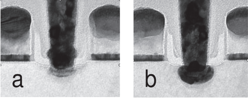
Figure 0186b clearly illustrates poor NiSi formation beneath the contact on the high-resistance side compared to proper NiSi formation at a reference site. Note
[1] Z. Song, SRAM failure analysis evolution driven by technology scaling, Proceedings of the 21th International Symposium on the Physical and Failure Analysis of Integrated Circuits (IPFA), DOI: 10.1109/IPFA.2014.6898207, 2014.
|