Chapter/Index: Introduction | A | B | C | D | E | F | G | H | I | J | K | L | M | N | O | P | Q | R | S | T | U | V | W | X | Y | Z | Appendix
| The most commonly reported failure mode in the literature after short-circuit exposure is gate oxide breakdown [1]. This is indicated by a reduction in the gate-source voltage during the on-state, caused by an increase in gate leakage current. This failure mode is attributed to the high temperature and electric field stress experienced by the thin gate oxide. In SiC MOSFETs, a thinner oxide layer is used to reduce channel resistance [2], enabling the design of robust short-circuit devices. Figure 0468a provides a statistical distribution of failure modes reported in literature for 1.2 kV SiC devices tested under short-circuit conditions with a 600 V DC-bus voltage. This chart highlights the proportion of different failure mechanisms observed during testing. The most prevalent failure mode is gate-oxide breakdown, accounting for a significant portion (62%) of the failures. This breakdown is primarily caused by high electric fields and temperatures that stress the thin gate oxide layer used in these devices. Other failure mechanisms include thermal runaway, which is triggered by a sudden rise in temperature within the device. This thermal runaway can result in local hot spots and eventual destruction of the device due to uneven current distribution and the activation of parasitic structures like the body diode and bipolar junction transistor (BJT).
Figure 0468b shows a gate breakdown failure for a power module (M4) at room temperature.
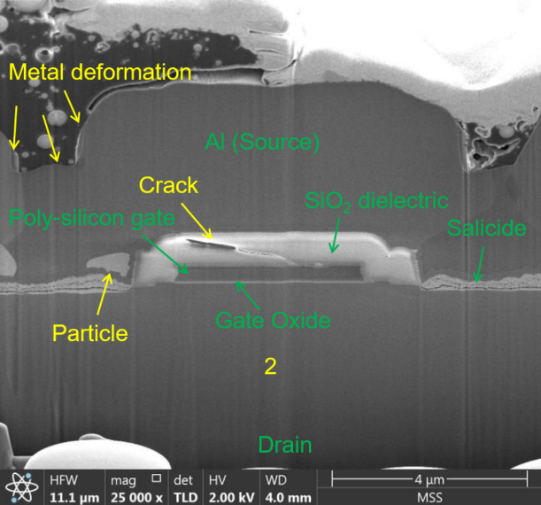
On the other hand, the SiC/SiO2 interface faces several challenges compared to traditional Si/SiO2 interfaces. First, the large bandgap of SiC increases tunneling currents through the gate oxide, resulting in higher gate leakage currents at the same oxide field for SiC/SiO2 interfaces. Second, the high blocking capability of SiC devices necessitates limiting the electric field in the gate oxide. This is achieved by implanting deep p-regions beneath the gate oxide and restricting the negative gate voltage in blocking mode. Third, SiC's high defect density contributes to extrinsic defects in the gate oxide, such as substrate defects, particle inclusion, and process variations. Recent physical inspections of damaged SiC MOSFETs have revealed cracks in the field oxide between the gate poly-silicon and the source contact, as well as melted aluminum. However, no damage to the gate oxide has been observed, as noted in prior studies. Figure 0468c shows that a short-circuit testing resulted in the formation of cracks between the poly-silicon gate and the aluminum source, metal particles near the source contact, and alterations in the top surface of the aluminum source. These defects were correlated with the increase in both gate-leakage and drain-leakage currents. The experimental condition that induced those defects in the SiC power MOSFETs was the short-circuit stress event. Specifically, the device was subjected to high junction temperatures and nominal voltages, which led to the degradation of the SiC MOSFETs.
Figure 0468d shows a SEM view of degraded and non-degraded cells near source wire bonding. The cells near the source wire bonds are most affected.
[1] L. Ceccarelli, P.D. Reigosa, F. Iannuzzo, F. Blaabjerg, A survey of SiC power MOSFETs short-circuit robustness and failure mode analysis, Microelectronics Reliability, 76–77, 272-276, 2017.
|