Chapter/Index: Introduction | A | B | C | D | E | F | G | H | I | J | K | L | M | N | O | P | Q | R | S | T | U | V | W | X | Y | Z | Appendix
| The power semiconductor market is growing rapidly due to increased demand for energy-efficient devices and the rise of renewable energy, electric vehicles, and smart grid systems. Valued at $34.9 billion USD in 2020, it’s expected to reach $44.2 billion USD by 2025, with a 4.8% CAGR (Compound Annual Growth Rate). Silicon carbide (SiC) is a key technology driving this growth, offering superior electric field strength, thermal conductivity, and faster switching speeds compared to silicon. SiC-based devices like MOSFETs and Schottky diodes are gaining traction in EVs, renewables, and high-voltage power transmission. Silicon Carbide (SiC) MOSFETs are considered wide-bandgap (WBG) semiconductor devices, meaning they have a wider bandgap compared to traditional silicon (Si) semiconductors. This wider bandgap gives them several advantageous properties over their silicon material:
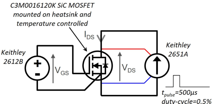
Figure 0807a illustrates the static characterization setup used to analyze the behavior of the 1.2 kV SiC MOSFET. The setup consists of two source-meter units (SMUs): the Keithley 2651A power SMU, which provides drain current pulses up to 50 A and measures the drain voltage with Kelvin sense wires, and the Keithley 2612B SMU, which biases the gate at the desired voltage level. The current pulses are set to a duration of 500 µs with a 0.5% duty cycle to prevent junction self-heating. The gate voltage is incremented in steps from -4 V to +15 V, with the transistor mounted on a temperature-controlled heat sink. This setup allows for precise measurement of the I-V characteristics under different gate-source voltages.
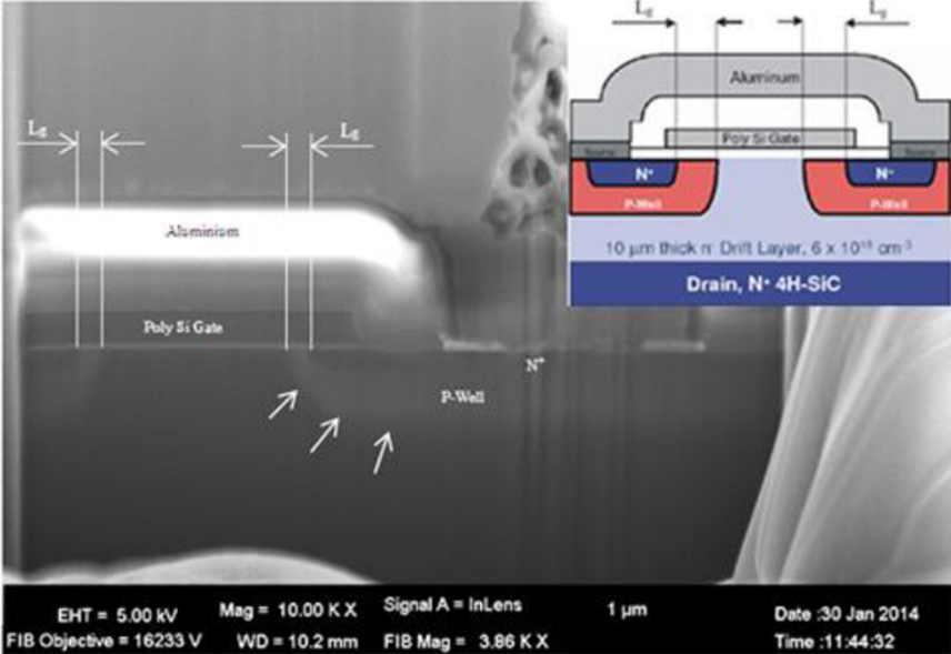
Figure 0807b shows the cross section of a SiC MOSFET cell. The device is a 1.2 kV vertical DIMOS SiC-MOSFET, designed with a nominal maximum drain current (IDmax) of 24 A at 25 °C [3]. Its architecture consists of multiple elementary cells arranged in parallel. The source electrode, made from aluminum, fully covers the top surface except for the gate bonding wire pad. The die is brazed onto a copper base plate, which facilitates heat dissipation, preventing excessive self-heating during electrical conduction. The brazing material, composed of an alloy of tin, silver, and antimony, has a maximum operating temperature of 260 °C.
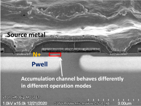
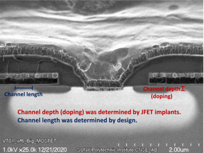
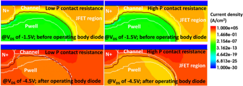
Figure 0807c (a) shows the cross-sectional SEM image of 1.2 kV accumulation channel mode MOSFETs. Forward conduction channel with strong accumulation of electrons is formed when Vgs is larger than Vth. P contact resistance in Figure 0807c (c) refers to the resistance at the contact between the P-type material (the heavily doped P-well) and the metal in the MOSFET. This resistance affects the current flow through the P-type regions, especially in conditions where the body diode of the MOSFET is conducting. Lower P contact resistance allows for better current conduction and results in higher current density from the P contact.
[1] Yi, P., Murthy, P. K. S., & Wei, L. “Performance evaluation of SiC
MOSFETs with long power cable and induction motor”. Energy
Conversion Congress and Exposition (ECCE), 2016.
|