| The Entire Block Failure in SRAM is a type of failure pattern where an entire block of SRAM cells fails. This pattern does not display any specific alignment with word line (WL) or bit line (BL) patterns, making it challenging to trace the exact location of the defect. To narrow down the defective area, Photon Emission Microscopy (PEM) analysis is often employed. In the document example, PEM analysis identified consistent emission in a specific circuit area across multiple failing chips, suggesting a systematic defect. Subsequent physical analysis then revealed broken polysilicon at these emission sites, pinpointing the defect's physical origin.
For instance, the procedure for troubleshooting Entire Block Failure in SRAM can involve the following steps:
- Identify the Failure Pattern: Since entire block failures, e.g. the failure shown in Figure 0888a, lack specific WL or BL patterns, the analysis begins with mapping the failed areas to understand if there are any consistent patterns across chips.

Figure 0888a. Wafer map displaying multiple entire block failures with a detailed chip-level failure bitmap on the right side. [1] |
-
PEM Analysis: Use Photon Emission Microscopy (PEM) to inspect multiple failing chips. PEM is particularly useful as it identifies regions with abnormal photon emissions, which often correlate with defect sites. In the example discussed, PEM analysis revealed emissions in a repeated specific circuit across the failing chips, which was absent in reference (non-failing) chips, as shown in Figures 0888b and 0888c.
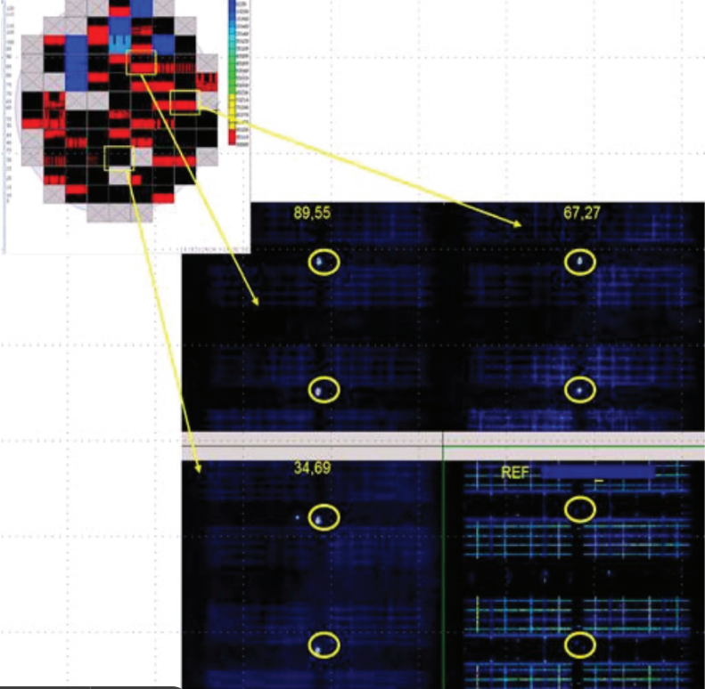
Figure 0888b. PEM image displaying emission sites at a recurring circuit location across three failing chips, with no emission detected at the corresponding circuit in a reference chip. [1] |
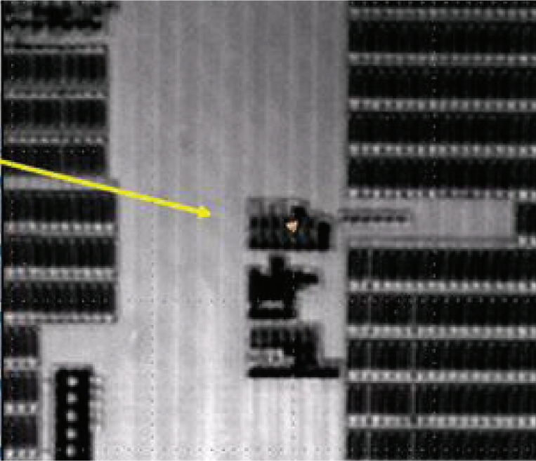
Figure 0888c. 100X PEM image showing one of the emission sites from Figure 0888b. [1] |
-
Verify the Emission Consistency: Confirm that the emission sites are consistent across different failing chips. Consistency in emission at particular circuits across multiple chips strongly suggests a systematic defect.
-
Focused Physical Analysis: Once PEM identifies the defective area, physical failure analysis is conducted specifically at the emission sites. This step includes de-processing the chip layer by layer if necessary and using SEM (Scanning Electron Microscopy) to observe the structures at emission sites.
-
Locate Physical Defects: In the documented case, SEM analysis at the emission sites identified broken polysilicon structures, as shown in Figure 0888d, which were the root cause of the entire block failure. Such defects in the polysilicon affect circuit continuity, leading to failure across the entire block.

Figure 0888d. SEM image illustrating a polysilicon fracture example. [1] |
By combining PEM for initial localization with SEM for detailed physical analysis, this procedure efficiently isolates and identifies the root cause of entire block failures in SRAM.
[1] Z. Song, SRAM failure analysis evolution driven by technology scaling, Proceedings of the 21th International Symposium on the Physical and Failure Analysis of Integrated Circuits (IPFA), DOI: 10.1109/IPFA.2014.6898207, 2014.
|
