Chapter/Index: Introduction | A | B | C | D | E | F | G | H | I | J | K | L | M | N | O | P | Q | R | S | T | U | V | W | X | Y | Z | Appendix
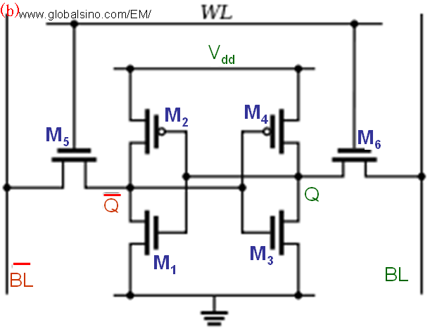
| Static random-access memory (SRAM or static RAM) is a type of semiconductor memory that uses bistable latching circuitry to store information. SRAM is a digital component. It operates with binary data—storing bits as either a '0' or '1'—and its internal circuits consist of transistors arranged to form bistable latches, which inherently function digitally. The digital nature of SRAM lies in its function and design. Unlike analog components, which handle a continuous range of values, SRAM stores discrete binary information, making it a key component in digital systems for fast, volatile storage. In "static RAM", the term "static" refers to the memory's ability to retain stored data as long as power is supplied, without needing to refresh the data periodically; therefore, such SRAM cell does not require any clock for operation. A typical SRAM bit cell contains of 4–8 transistors. In modern technology nodes, particularly those used in high-performance processors, SRAM instances are frequently employed due to their speed and efficiency in storing small amounts of data that can be accessed rapidly. These microchips often contain millions of such SRAM cells, which are integrated into various functional blocks (or tiles) across the chip. The tiles may serve different purposes, such as computation or data handling, and the SRAM configurations within them vary in design and size depending on the specific function. For example, some tiles may use smaller, more compact SRAM arrays for temporary data storage, while others might use larger or more specialized SRAM instances optimized for speed or power consumption. This widespread and varied use of SRAM is crucial for the performance and efficiency of modern CPUs and GPUs, which need fast, localized memory to support high computational loads. In SRAMs, a single word-line is divided into several ones by the sub-wordline drivers (SWL). Every SWL has to be selected by the main word-line (MWL) and the row select line signal (RX). Thus, only a partial word-line will be activated. Figure 1109a shows a six-transistor CMOS SRAM bit cell. Each bit in an SRAM is stored on the four transistors (M1, M2, M3, and M4) that form two cross-coupled inverters. This storage cell has two stable states (0 and 1). Two additional access transistors (M5 and M6) control the access to the storage cell during read and write operations.
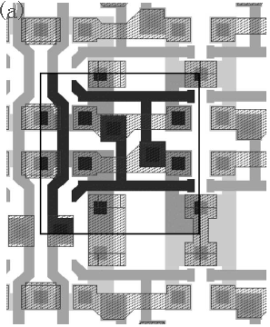
Figure 1109b shows the typical layout of an SRAM cell with 6 transistors and 12 contacts, depicted in Figure 1109a, but presented in a different way.
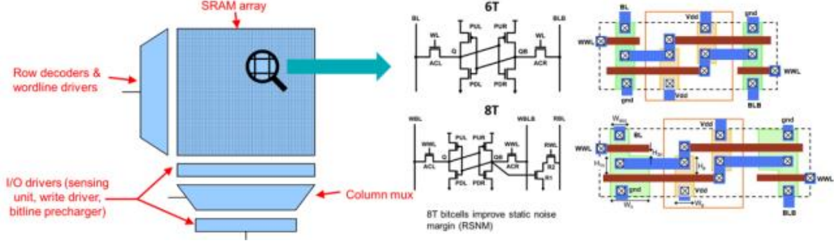
Figure 1109c shows the schematic design of a typical SRAM array layout, depicting the structure of 6-transistor or 8-transistor memory cells organized across the array. This configuration is essential for diagnosing and characterizing defects as it allows for detailed spatial mapping of failure patterns within the SRAM. By examining the array layout, specific fail signatures can be correlated to Front-End of Line (FEOL) and Middle-End of Line (MEOL) layer defects, which are present in zones containing critical transistor structures and interconnections. The layout scheme illustrated in Figure 1109c serves as a foundation for analyzing SRAM bitmap data, facilitating insights into yield improvement strategies by identifying defect clusters and their potential root causes across various process layers.
[1] Alex A. Volinsky, Larry Rice, Wentao Qin, and N. David Theodore, FIB failure analysis of memory arrays, Microelectronic Engineering 75 (2004) 3–11.
|