Integrated Circuits and Materials

An Online Book, First Edition by Dr. Yougui Liao (2018)

Practical Electron Microscopy and Database - An Online Book

Chapter/Index: Introduction | A | B | C | D | E | F | G | H | I | J | K | L | M | N | O | P | Q | R | S | T | U | V | W | X | Y | Z | Appendix

Inverter (NOT Gate) Design in Logic ICs

An inverter, or NOT gate, is a digital logic gate that performs logical negation by outputting the opposite of its input bit, typically represented by two voltage levels. When the input is 1, the output is 0, and vice versa, a process commonly referred to as "flipping" bits. The NOT gate is equivalent to the logical negation operator (¬) in mathematics, making it a unary operation with a simple truth table. Also known as the complement gate, it produces the ones' complement of a binary number by swapping 0s and 1s. That is, an inverter circuit functions as a fundamental logic gate that switches between two voltage levels. Along with AND and OR gates, the NOT gate is one of the three fundamental logic gates from which any Boolean function can be constructed.  

Inverter (NOT gate) design

Figure 1460a. Inverter (NOT gate) design.

Inverter circuits come in several different forms depending on the technology and application:
  • CMOS Inverter:
    • Uses complementary MOSFETs (both nMOS and pMOS transistors) to implement the inverter. This is the most commonly used inverter in modern digital circuits because of its low power consumption.
      NMOS Inverter
      inverter layout
      (a)
      (b)
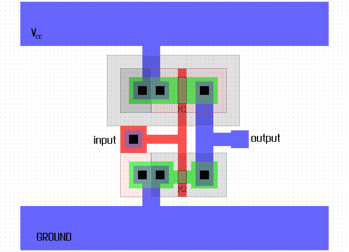
    Figure 1460b. CMOS Inverter: (a) Circuit, and (b) Layout.

    CMOS Inverter is the most fundamental and widely used one.

  • PMOS Inverter:
NMOS Inverter
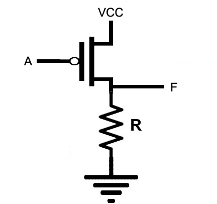
Figure 1460c. PMOS Inverter.

Figure 1460c shows pMOS Transistor, which is connected to the positive voltage supply (Vcc). When the input is low (logic 0), the pMOS transistor is ON, allowing current to flow from Vcc to the output, which becomes high (logic 1).
  • NMOS Inverter:
    • As shown in Figure 1460d, it uses only nMOS transistors, typically an nMOS transistor with a resistor pull-up. This was common in older technologies but consumes more power than CMOS.

      NMOS Inverter

      Figure 1460d. NMOS Inverter.

      In this case, the nMOS transistor is connected to ground (0V). When the input (A in Figure 1460d) is high (logic 1), the nMOS transistor is ON, allowing current to flow from the output to ground, making the output low (logic 0).

  • BJT Inverter:
    • Uses a single bipolar junction transistor (BJT) with a resistor to create an inverting operation.
  • TTL Inverter:
    • Based on bipolar junction transistors (BJTs), commonly used in older transistor-transistor logic (TTL) circuits.


[1] https://www.sccs.swarthmore.edu/users/06/adem/engin/e77vlsi/lab3/.