Chapter/Index: Introduction | A |
B |
C |
D |
E |
F |
G |
H |
I |
J |
K |
L |
M |
N |
O |
P |
Q |
R |
S |
T |
U |
V |
W |
X |
Y |
Z |
Appendix
Wide-Bandgap (WBG) Power Semiconductors: SiC and GaN
| Wide-bandgap (WBG) power semiconductors such as Silicon Carbide (SiC) and Gallium Nitride (GaN) enable faster switching speeds compared to traditional semiconductors like silicon (Si). This is primarily due to their superior material properties, particularly their higher critical electric field strength (breakdown field), faster electron saturation
velocity, higher thermal conductivity, and lower intrinsic carrier concentration:
- Higher Breakdown Electric Field:
- WBG materials have higher critical electric fields compared to silicon, which allows them to tolerate higher voltages for the same thickness of material. This means WBG devices can be made with thinner drift regions, which results in lower on-resistance (Ron) and faster switching speeds because of reduced capacitance and stored charge.
- The one-dimensional approximation of breakdown voltage can be given by,
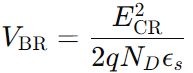 ----------------------------- [1629a] ----------------------------- [1629a]
where,
-
Lower Parasitic Capacitances:
- The lower intrinsic capacitance due to a thinner depletion region in WBG devices allows for faster charging and discharging during switching, reducing the switching losses and allowing for higher switching frequencies.
- The capacitance can be given by,
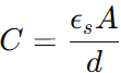 ----------------------------- [1629b] ----------------------------- [1629b]
where,
C is the capacitance.
A is the area.
d is the distance between the plates, which corresponds to the thickness of the depletion region.
- Lower Carrier Lifetime:
- WBG semiconductors have lower intrinsic carrier concentrations and shorter minority carrier lifetimes compared to silicon, which leads to reduced switching losses and faster recovery times in devices such as diodes.
- The minority carrier lifetime can be given by,
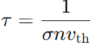 ----------------------------- [1629c] ----------------------------- [1629c]
where,
-
Higher Thermal Conductivity:
- WBG materials have higher thermal conductivity, allowing them to handle more power and operate at higher junction temperatures. This reduces the thermal constraints on switching speed, as heat is more effectively dissipated.
- The thermal conductivity can be given by,
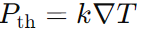 ----------------------------- [1629d] ----------------------------- [1629d]
where,
Pth is the thermal power.
k is the thermal conductivity of the material.
∇T is the temperature gradient.
Table 1629. Comparison of the key properties of Silicon (Si), Silicon Carbide (SiC), and Gallium Nitride (GaN).
| Material |
Critical Electric Field (ECR) |
Electron Mobility |
Hole Mobility |
Thermal Conductivity (k) |
Bandgap (Eg) |
Intrinsic Carrier Concentration (ni) |
Maximum Junction Temperature (Tj) |
| Silicon (Si) |
0.3 MV/cm |
1400 cm2/Vs |
600 cm2/Vs |
1.5 W/cm·K |
1.1 eV |
1.5 × 1010 cm-3 |
~150°C |
| Silicon Carbide (SiC) |
2.8 MV/cm |
900 cm2/Vs |
100 cm2/Vs |
4.9 W/cm·K |
3.26 eV |
10 cm-3 |
~300°C |
| Gallium Nitride (GaN) |
3.3 MV/cm |
1250 cm2/Vs |
200 cm2/Vs |
1.3 W/cm·K |
3.4 eV |
1 cm-3 |
~400°C |
|
