Chapter/Index: Introduction | A | B | C | D | E | F | G | H | I | J | K | L | M | N | O | P | Q | R | S | T | U | V | W | X | Y | Z | Appendix
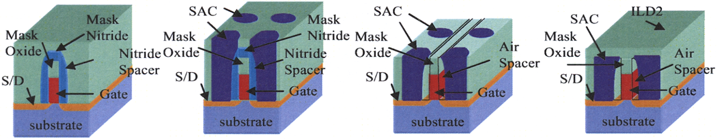
| In semiconductor scaling, interlayer dielectric (ILD) materials play a crucial role in isolating various layers of interconnects, especially as technology nodes shrink. Initially, aluminum was used for metallization with thicker ILD layers, but as technology advanced, copper replaced aluminum, and thinner ILD materials, like low-k SiCOH, were introduced to reduce parasitic capacitance and improve performance. This evolution in ILD materials has required adaptations in failure analysis techniques. Earlier methods relied on etching, which could introduce artificial defects. In contrast, advanced nodes use parallel polishing and backscattered electron (BSE) imaging for more precise defect localization without damaging the sample. The BSE imaging, advantageous for its depth and atomic number contrast, allows for clearer imaging of defects within ILD, especially for structures with high atomic number contrasts, such as copper or tungsten interconnects in low-k ILD matrices. Furthermore, the thickness of ILD layers has reduced, and new materials have been introduced, prompting advancements in physical failure analysis methods. Figure 2262a shows the process flow ofthe novel air-spacer SAC transistor. Figure 2262a(b) shows that SAC has been formed by high-selectivity contact hole etch and contact plug filling. Figure 2262a (c) shows the CMP step to expose the top of the mask nitride and selective etch of the nitride mask and spacer without etching the oxide to create an air gap. Figure 2262a (d) shows non-conformal ILD2 deposition has sealed the top openings and then completed the air spacers.
Borophosphosilicate glass (BPSG) has been used for the premetal dielectric (PMD) or interlayer dielectric (ILD) to reduce the required reflow temperature. A thin layer of silicon nitride is commonly used for copper metallization as an ILD etch-stop layer (ESL). Materials used as interlayer dielectric (ILD) layers are:
Figure 2262b. Schematic cross section of BEOL. [2] These LPCVD highly boron-containing glasses can be used only for the first level of ILD, even though such glasses with low polarizability are favorable for the device planarization in DRAMs and static random access memory (SRAMs) cells. The reason is that that even the low temperature reflow glasses would melt the metal once deposited as the standard temperature of reflow far exceeds melting point of aluminum. On the other hand, high temperatures are unsuitable for other metals due to diffusion and electro-migration issues. Furthermore, due to void formation during reflow as shown in Figure 2262c, and very high thermal budget, the process of doped glass reflow is not a very widely implemented process of planarization.
[1] Jemin Park and Chenming Hu, Air spacer MOSFET technology for 20nm node and beyond, 2008 9th International Conference on Solid-State and Integrated-Circuit Technology, DOI: 10.1109/ICSICT.2008.4734461, (2008).
|
||||||||||