Chapter/Index: Introduction | A | B | C | D | E | F | G | H | I | J | K | L | M | N | O | P | Q | R | S | T | U | V | W | X | Y | Z | Appendix
| Self-Aligned Quadruple Patterning (SAQP) is an advanced lithography technique used to achieve extremely fine pattern resolutions, particularly for sub-20nm nodes. SAQP builds on the concept of Self-Aligned Double Patterning (SADP), utilizing a resist-core-based scheme that allows for pitch quadrupling, essential for manufacturing very dense integrated circuits. In SAQP, a resist pattern is initially used to create spacers that double the line density, similar to SADP. Then, an additional set of spacers is deposited and patterned over the previous set, effectively quadrupling the initial pitch. This process is achieved by carefully controlling each layer and ensuring accurate alignment, which is critical for achieving high-resolution features down to 11nm half-pitch as demonstrated in recent implementations. This method relies on low-temperature deposition materials, such as SiO2, which enhance patterning precision and reduce critical dimension (CD) variability. Figure 2352a shows two different self-aligned quadruple patterning (SAQP) processes. The Two Hard Mandrels Process, shown in Figure 2352a (a), involves using two distinct mandrels to achieve precise, high-resolution patterning on a substrate. In this method, the patterned structures are defined by placing spacer layers onto hard mandrel templates, which serve as physical guides for the deposition process. Plasma-assisted atomic layer deposition (ALD) is used to deposit the spacers, typically made of SiO2, due to its ability to create conformal, high-quality films with excellent thickness control even on complex topographies. The use of SiO2 spacers ensures durability and stability, as this material is resistant to common etching processes used in subsequent steps. By relying on two hard mandrels and a sequential ALD approach, this technique effectively doubles the pattern density without additional lithography steps, making it particularly valuable for scaling down feature sizes in advanced semiconductor devices. In this SAQP method, the hard mandrels are usually composed of materials such as amorphous silicon (a-Si) or other silicon-based compounds, chosen for their compatibility with the plasma ALD process and ability to withstand etching and deposition without deforming. The stability of these materials ensures that the mandrels maintain precise pattern fidelity during spacer deposition, which is crucial for achieving the intended device architecture in advanced semiconductor manufacturing. On the other hand, the spacer-on-spacer process, shown in Figure 2352a (b), is a SAQP technique that utilizes two distinct spacer materials in sequence to achieve high-density patterning required in advanced semiconductor manufacturing. In this approach, the first spacer, typically silicon dioxide (SiO2), is deposited conformally over the initial mandrel structure, forming precise sidewall coatings. After this, the first spacer is used as a mask, and a second spacer layer, such as titanium dioxide (TiO2), is applied over the initial pattern. This dual-layer approach is essential in achieving extremely fine feature sizes, as the differing material properties of each spacer help in maintaining distinct and stable boundaries during subsequent etching steps. Plasma-assisted ALD is used to deposit these spacers, leveraging its high precision and conformal coating capabilities to ensure consistent layer thickness even on complex topographies. The spacer-on-spacer technique thus enables further miniaturization in device manufacturing, accommodating the need for increasingly smaller and more densely packed features as technology advances.
The transmission electron microscopy (TEM) images in Figure 2352b illustrate the stages of SAQP, shown sequentially from left to right: initial patterning of the first core onto a mandrel; SiO2 deposition via atomic layer deposition (ALD); etching of the first set of spacers; mandrel etching to create the second core; additional SiO2 deposition by ALD; and, finally, etching of the second spacers and the silicon nitride pad.
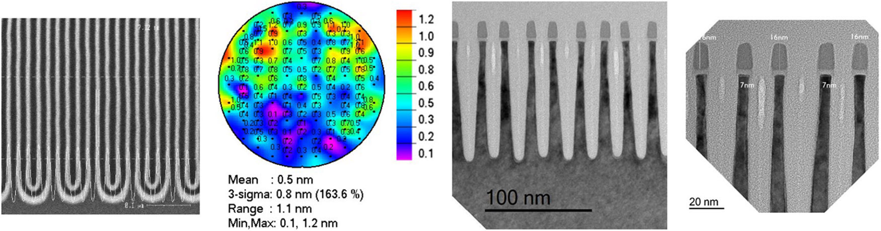
Figure 2352c illustrates key visual data from the SAQP process, presented in Figure 2352b, providing insights into fin pattern uniformity and dimensional accuracy. The left panel presents a CDSEM image of the patterned fins, showing the effects of etching and wet cleaning with hydrofluoric acid (HF), which sharpens the structural definition of the fins. Moving to the center, a contour map visualizes the pitch walk, quantitatively capturing deviations across the entire wafer. This map enables precise analysis of pitch variation post-SAQP. In the right panel, TEM images reveal the final fin structure after etching and HF cleaning. Voids observed in these TEM samples, a result of sample preparation, subtly alter the fins’ appearance, suggesting a careful consideration of void formation effects in assessing the pattern's structural integrity.
[1] Knoops, H. C. M., Faraz, T., Arts, K., & Kessels, W. M. M. (2019). Status and prospects of plasma-assisted atomic layer deposition. Journal of Vacuum Science & Technology A, Vacuum, Surfaces, and Films, 37(3), 030902. https://doi.org/10.1116/1.5088582.
|
|||||||||||||||||||||||