Bit Line Contact (BLC) in DRAM - Integrated Circuits and Materials - - An Online Book - |
||||||||
| Integrated Circuits and Materials http://www.globalsino.com/ICsAndMaterials/ | ||||||||
| Chapter/Index: Introduction | A | B | C | D | E | F | G | H | I | J | K | L | M | N | O | P | Q | R | S | T | U | V | W | X | Y | Z | Appendix | ||||||||
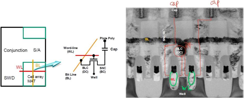
================================================================================= In DRAM, bitline contacts and digit contacts often refer to the same thing. The terms can be used interchangeably, depending on the context and the specific naming conventions of different manufacturers or design documents. The terminology can vary because of historical reasons, design preferences, or specific conventions adopted by different companies or publications. However, the fundamental function they describe remains the same: connecting the bitlines to the memory cells in the DRAM array. Figure 2375a shows DRAM 8F2 cell structure:
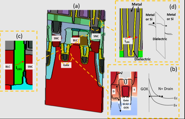
Figure 2375a. DRAM 8F2 cell structure. [1] Figure 2375b shows the three main leakages in DRAM cells.
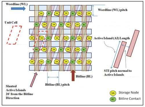
Figure 2375c. Cell Layout of a Samsung DRAM using the buried wordline (bWL). Adapted from [3] ============================================
[1] https://blog.naver.com/minky0118/221860772321.
|
||||||||
| ================================================================================= | ||||||||
|
|
||||||||