Electron microscopy
 
Cell Array MAT in DRAM
- Integrated Circuits and Materials -
- An Online Book -
Integrated Circuits and Materials                                                                                  http://www.globalsino.com/ICsAndMaterials/        


Chapter/Index: Introduction | A | B | C | D | E | F | G | H | I | J | K | L | M | N | O | P | Q | R | S | T | U | V | W | X | Y | Z | Appendix

=================================================================================

In DRAM (Dynamic Random Access Memory), a "mat" refers to a subarray or a smaller array within the larger DRAM chip. Here are some details about what a mat is and its significance in DRAM design: 

  • Definition and Structure
    • Mat: A mat in DRAM is a subdivision of the DRAM array. Each DRAM chip is divided into several mats, which are further organized into rows and columns of memory cells.
    • Subarray: The term "subarray" is often used interchangeably with "mat." It signifies a smaller, manageable portion of the entire memory array, designed to facilitate easier access and control.
  • Purpose and Benefits
    • Localized Access: Mats enable localized access to smaller sections of the DRAM, which can improve access times and reduce power consumption.
    • Redundancy and Yield: By dividing the DRAM into mats, manufacturers can implement redundancy more effectively. If a defect is found in one mat, it can be replaced with a redundant mat, improving the overall yield and reliability of the DRAM chip.
    • Hierarchical Organization: Mats are part of a hierarchical organization that includes banks, rows, and columns. This hierarchy helps in efficient addressing and management of the memory.
    • Parallelism: Multiple mats can be accessed in parallel, enhancing the data throughput and performance of the DRAM.
  • Hierarchical Structure in DRAM
    • Bank: A bank is a larger division within a DRAM chip, containing multiple mats.
    • Mat: Each mat is a subarray within a bank, consisting of a specific number of rows and columns of memory cells.
    • Row and Column: Within each mat, the memory cells are arranged in rows and columns, which are accessed using wordlines and bitlines.

Consider a DRAM chip with multiple banks, where each bank contains several mats. When a read or write operation is initiated, the memory controller selects the appropriate bank and mat, and then accesses the specific row and column within the selected mat as shown in Figure 2376a.

Visual representation of banks, mats, and rows

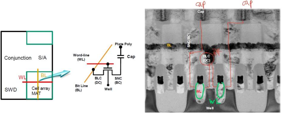
Figure 2376a. Visual representation of banks, mats, and rows.

Figure 2376b shows DRAM 8F2 cell structure:
        S/A -- Sense amplifier.
        WL -- Word-line.
        BL -- Bit-line.
        BLC -- Bit line contact.
        SNC -- Storage node contact.
        Cap -- Capacitor.

DRAM cell structure

Figure 2376b. DRAM 8F2 cell structure. [1]

In the DRAM bank organization shown in Figure 2376c, a DRAM bank is divided into multiple subarrays [3, 4, 5]. Each subarray comprises mul- tiple wordline drivers and sense ampliers (SAs). Subarrays are further divided into DRAM MATs. DRAM MATs are separated from each other by wordline (WL) drivers that are activated to drive a DRAM wordline within the DRAM MAT. In a DRAM MAT, DRAM cells are organized into a two-dimensional structure over bitlines and wordlines. The set of cells over the same wordline forms a DRAM row. 

DRAM subarray, MAT, row and cell organization

Figure 2376c. DRAM subarray, MAT, row and cell organization. [2]

Figure 2376c shows a DRAM MAT with the hierarchical wordline design.  In the hierarchical wordline design, a DRAM row address is partitioned into two pieces. The higher-order bits of the row address are used to select and activate a master wordline (MWL). The MWL is connected to four local wordline (LWL) drivers (D0, D1, D2, D3 in Figure 3) that are used to activate four consecutive DRAM rows in a MAT. The least significant two bits of the row address are used to assert one of the four LWL select lines (S0 to S3) to enable an LWL driver and finally activate a DRAM row. An activated MWL potentially drives four consecutive LWLs that form a segment. We hypothesize that the QUAC command sequence (ACT-PRE-ACT) asserts S0 to S3 approximately at the same time, resulting in the simultaneous activation of four consecutive DRAM rows.

DRAM subarray, MAT, row and cell organization

Figure 2376c. DRAM MAT with hierarchical wordlines. [2]


============================================


[1] https://blog.naver.com/minky0118/221860772321.
[2] Ataberk Olgun, Minesh Patel, A. Giray Yağlıkçı, Haocong Luo, Jeremie S. Kim, F. Nisa Bostancı, Nandita Vijaykumar, Oğuz Ergin, and Onur Mutlu, QUAC-TRNG: High-Throughput True Random Number Generation Using Quadruple Row Activation in Commodity DRAM Chips, A shorter version of this work is to appear at the 48th IEEE International Symposium on Computer Architecture (ISCA 2021), https://doi.org/10.48550/arXiv.2105.08955, 2021 (v1).
[3] K. K. Chang et al., “Improving DRAM Performance by Parallelizing Refreshes with Accesses,” in HPCA, 2014.
[4] Y. Kim et al., “A Case for Exploiting Subarray-level Parallelism (SALP) in DRAM,” in ISCA, 2012.
[5] V. Seshadri and O. Mutlu, “In-DRAM Bulk Bitwise Execution Engine,” arXiv:1905.09822, 2020.


=================================================================================