8F2, 6F2 and 4F2 - Integrated Circuits and Materials - - An Online Book - |
||||||||
| Integrated Circuits and Materials http://www.globalsino.com/ICsAndMaterials/ | ||||||||
| Chapter/Index: Introduction | A | B | C | D | E | F | G | H | I | J | K | L | M | N | O | P | Q | R | S | T | U | V | W | X | Y | Z | Appendix | ||||||||
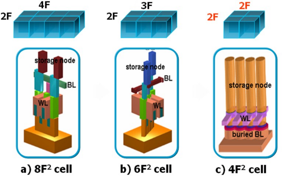
================================================================================= F is the feature size of the process technology. Feature size is either the minimum distance between the source and drain on a MOS transistor or half the distance between cells in a DRAM chip (known as "DRAM half pitch"). DRAM cell sizes are then measured using an nF2 formula where n is a constant. Bit sizes are measured in F2, which is the smallest feature you can create. The cell architecture shown in Figure 2380a has been evolved from 8F2 cell to 6F2 cell since the cell size could be reduced up to 75% at the same design rule (F). [1]
Figure 2380b shows DRAM 8F2 cell structure:
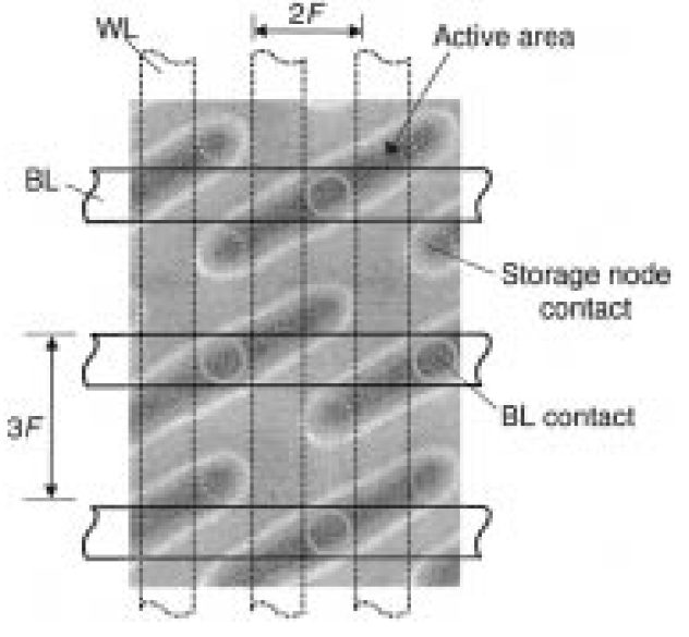
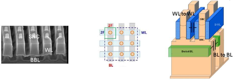
Figure 2380b. DRAM 8F2 cell structure. [2] DRAM cells have used an 8F2 architecture for many years. This design allows for the use of a folded bitline architecture, which helps reduce noise. [5] Comparing with 6F2, due to larger cell size, the 8F2 layout has two major advantages: However, 6F2 cells can be used to decrease cell area with the same WL and BL pitchs. Figure 2380c shows the top view of a 6F2 cell, which is estimated as the simplest structure of the COB cells. This 6F2 cell has a 3F bitlines pitch and 2F wordlines pitch.
Figure 2380c. DRAM 6F2 cell. [3] Driving toward 4F2 cell size can further improve bit density and to lower production cost.
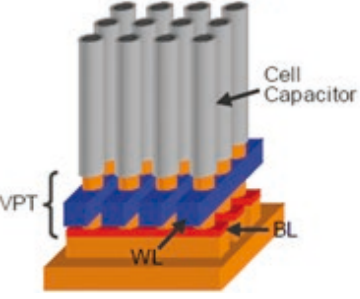
Figure 2380d. DRAM 4F2 VCAT cell structure. [2]
============================================
[1] Yoosang Hwang, Jemin Park, Gyo-Young Jin, Chilhee Chung, An Overview and Future Challenges of High Density DRAM for 20nm and Beyond, the 2012 International Conference on Solid State Devices and Materials, Kyoto, 2012, pp586-587.
|
||||||||
| ================================================================================= | ||||||||
|
|
||||||||